Intel could be bringing its 56-core CPUs to workstations

mongeese

Posts: 643   +123
Staff
In context: Intel first announced the Sapphire Rapids line of Xeon processors in late 2019 and has released information about them at a trickle ever since. With up to 56 cores and in-package memory, they'll be Intel's most powerful and enormous processors to date.

Intel has been steadily updating the relevant enterprise software in preparation for Sapphire Rapids for over a year. Some of that software is open source and the source of small leaks. Last week, a trawler found a reference to an unknown processor in the boot log of a Linux kernel, the Intel W9-3495.

First, the name: Intel uses "W" for its workstation CPUs, for example, the W-3375. It hasn't put numbers after the "W" yet, so that could mean a few things, but it looks a lot like the nomenclature used by the Core series -- i5, i7, i9. It might imply the existence of similar W7 or W5 CPUs with lower core counts.

Second, the specs. The boot log says that the W9-3495 has 56 cores / 112 threads and a base clock of 1.8 GHz (that likely isn't final). It lists AMX and AVX-512 instructions as features of the CPU.
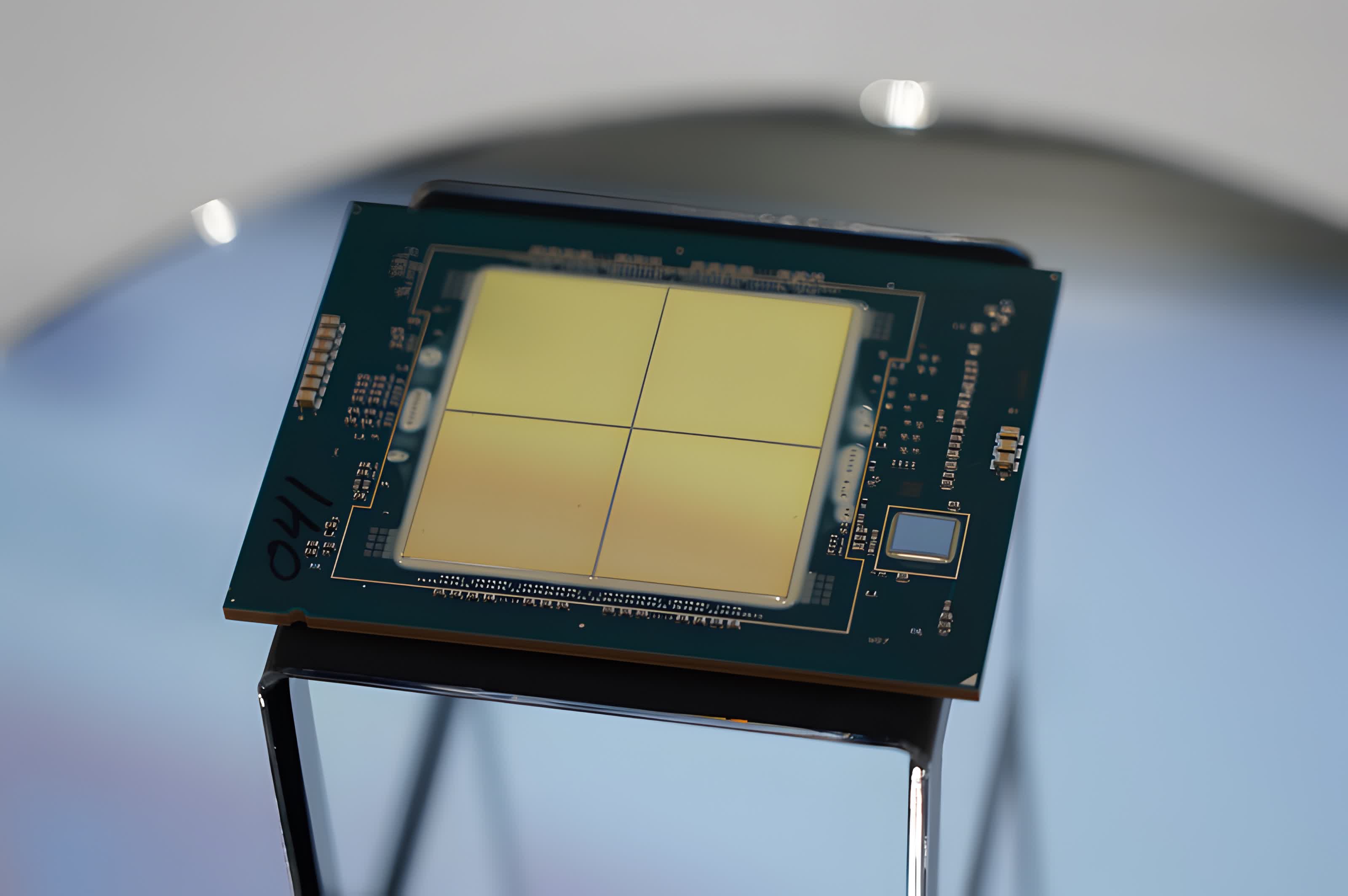
However, it doesn't say whether or not the W9-3495 has the 64 GB of in-package HBM2e memory that Sapphire Rapids has garnered infamy for, and I'd wager that it won't. It's prohibitively expensive, and also something that Intel would reserve for its flagship data center processors as a selling point.

Intel's workstation CPUs do usually have most of the features of their server-side counterparts, though. If the W9-3495 is no exception, then it will have eight lanes of DDR5 and a mix of PCIe 5.0 and PCIe 4.0 lanes summing to 80. It will definitely use the Willow Cove architecture and Intel 7 node (a rebrand of the 10nm Enhanced SuperFin Mouthful node) and the new LGA4677-X socket.

It will also be a mile above Intel's current offerings. Today's workstation flagship is the W-3375, which has only 38 cores / 76 threads and uses the Ice Lake architecture from late 2019 and the first-gen 10nm node. It's also stuck with DDR4 and PCIe 4.0. It costs a whopping $4,499 - ouch - and is only really available through OEMs, a fate that hopefully the W9-3495 can avoid.

Permalink to story.

 
So essentially this is a Zen 1 Threadripper MCM processor.

Referring to the Numa nodes / lack of IOD as these are multiple CPU tiles each with their own memory controller and IO.
 
So essentially this is a Zen 1 Threadripper MCM processor.

Referring to the Numa nodes / lack of IOD as these are multiple CPU tiles each with their own memory controller and IO.
are you talking about performance wise or architecture wise? Because the chiplet/tile idea has been around since the 80's, they just didn't have an interconnect that could give them the performance they wanted and making single dies was more economically feasible for the next 3 decades. I may be wrong, but I think it was IBM who came up with the first multiple chip design in 1982.

And to expand further on this, we had things like SLI and Crossfire, just to name a few, that are effectively a chiplet design with the interconnect being the limiting factor. IE, SLi cable or crossfire bridge. Then they moved to multiple GPUs on a single card, which also didn't work great.

With yields dropping at smaller nodes it suddenly made sense to invest in an interconnect that could give the performance they needed. It wasn't just the interconnect, it was the bridge and IO die managing resources at a hardware level to account for latency issues between chiplets/tiles. Looking at zen1, the major performance issue was from each chiplet having a direct connection to all other chiplets. Some chips had to make 2 jumps instead of 1 to share resources and this was the major change from ryzen 1000 to the 2000 series.

I maybe also be wrong about this, but I believe that the larger L3 cache sizes helped reduce the performance impact of having to share resources between chiplets
 
are you talking about performance wise or architecture wise? Because the chiplet/tile idea has been around since the 80's, they just didn't have an interconnect that could give them the performance they wanted and making single dies was more economically feasible for the next 3 decades. I may be wrong, but I think it was IBM who came up with the first multiple chip design in 1982.
I am talking MCM type (several multi purpose chiplets / tiles like Zen1 vs specialized ones like Zen 2 and later) and Numa node wise.

Yes, there‘s more cache and Foveros as interconnect but I would be very surprised if multi chiplet SPR did not have the same issues Zen 1 multi chiplet processors had back in 2017 with certain applications / games.

And tbh I am surprised Intel is releasing such a basic MCM design in 2022 or 23, I.e. five+ years later.
I haven' been able to dig up what the interconnect is like but I, too, would be surprised if they used something closer to Zen 1.
 
So, when are we going to see 8P+88E Xeon part?
you know, I was going to make a joke about that but at the same time, things like RaspPi cluster have shown themselves useful for many applications. However, we start blending the line between GPU's and CPUs at that point....However, there have been 128core ARM server CPUs that run at higher clocks than eypc or xeon. due to the nature of ARM cores being smaller than x86/x64cores I'm sure they will continue to have more cores per mm^2
 
Back