Nvidia Ampere vs. AMD RDNA 2: Battle of the Architectures

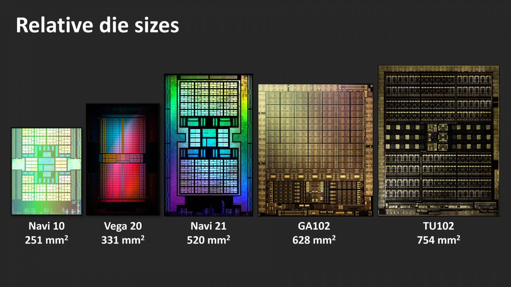
AMD has been using TSMC's much smaller N7 process since 2018... All of their Navi GPUs are made on the same process, so it makes to compare these products.
Isn't Navi21 being manufactured on N7P, not the original N7FF? Essentially a different node, with higher transistor densities.

[Ampere] supports a new feature called Fine-Grained Structured Sparsity and without going into the details of it all, essentially it means the math rate can be doubled.
Only a very specific type of math: operations on sparse matrices. Useful for ML apps, but I don't know that any game engines will benefit from this.

Anyway, an excellent overview in general of the two architectures.
 
Last edited:
I believe a word is missing in that last setence. And isn't Navi21 being manufactured on N7P, not the original N7FF? Essentially a different node, with higher transistor densities.
Yes it is N7P, but that process node doesn't offer higher transistor densities than N7, simply either lower power consumption for the same clocks or higher clocks for the same power. The higher density advancement is to be found with N7+. I'll tweak the article to make this a little clearer.

Only a very specific type of math: operations on sparse matrices.
Well the math is the same, just the nature of the matrix (I.e. there needs to be a number of zero-values within the matrix, in order to compress it).

Edit: It's actually only for a very specific sparsity pattern too - more can be read out it in this presentation by Nvidia:


The issue with finding a use for it in gaming is that the Tensor Cores in Ampere/Turing aren't being heavily used enough in games to warrant the need to try and mess about with sparsity.
 
Last edited:
Yes it is N7P, but that process node doesn't offer higher transistor densities than N7...The higher density advancement is to be found with N7+.
I meant N7+, sorry. Navi21's density is 51.5 mT/mm^2, whereas Navi10 was 20% lower. Some of that could be due to layering, obviously, but I thought AMD was taking advantage of the 15% density advantage that N7+ offers. Do you know if AMD (or TMSC) has made a definitive statement in this regard?
 
Do you know if AMD (or TMSC) has made a definitive statement in this regard?
Not a definitive one, as such, just that RDNA 2 is using the "same 7nm technology" (their words) as RDNA. This implies that it's still N7P.

The transistor density in Navi 21 is still quite a lot lower than what can be achieved with N7P (if one ignores anything to with layers) - the CDNA 1 Arcturus chip is 66.7 MT/mm2 and the Ampere GA100 is 65.6 MT/mm2; both over 27% higher than Navi 21.
 
"This value is set by the size of the base address register (BAR) and as far back as 2008, there has been an optional feature in the PCI Express 2.0 specification to allow it be resized. The benefit of this is that fewer access requests have to be processed in order to address the whole of the card's DRAM.
At present, the system is limited to Windows systems running a specific combination of Ryzen 5000 CPUs, 500 series motherboards, and Radeon RX 6000 graphics cards."

This is not exactly true. SAM has been supported by Linux for years on different AMD GPU and CPU combinations. Alex Deucher (Linux AMD driver developer) wrote:

"Smart Access Technology works just fine on Linux. It is resizeable BAR support which Linux has supported for years (AMD actually added support for this), but which is relatively new on windows. You just need a platform with enough MMIO space. On older systems this is enabled via sbios options with names like ">4GB MMIO"."
 
This is not exactly true. SAM has been supported by Linux for years on different AMD GPU and CPU combinations.
Hmmm, I had meant to say "...limited on Windows systems..." rather than "...limited to..."; I was aware of the support in Linux, but wasn't sure exactly what hardware and driver configurations support it.

Thanks for the feedback - I'll tweak that line accordingly.
 
"In Gears 5, for example, the Radeon RX 6800 (which uses a 60 CU variant of the Navi 21 GPU) only took a 17% frame rate hit, whereas in Shadow of the Tomb Raider, this rose to an average loss of 52%. In comparison, Nvidia's RTX 3080 (using a 68 SM GA102) saw average frame rate losses of 23% and 40% respectively, in the two games."
However, the quality of RT is different and so, such comparisons are flawed. By looking at side to side images (check it online), it is clear NVidia`s RT looks better, so it probably uses more computational power.

 
This is a fantastic insight folks, thanks for writing it!
Since you briefly go into media and codec support:
Can we see that area on the die shot? How large is it these days
 
Not a definitive one, as such, just that RDNA 2 is using the "same 7nm technology" (their words) as RDNA. This implies that it's still N7P.
Ok, I can accept that. However, if AMD is using 7nm DUV, and Apple's M1 is using N5, then which customers are using all of TSMC's 7nm EUV capacity?
 
This is a fantastic insight folks, thanks for writing it!
Since you briefly go into media and codec support:
Can we see that area on the die shot? How large is it these days
Here you go:

video.jpg

Ok, I can accept that. However, if AMD is using 7nm DUV, and Apple's M1 is using N5, then which customers are using all of TSMC's 7nm EUV capacity?
It was Huawei - not sure who now.
 
Ok, I can accept that. However, if AMD is using 7nm DUV, and Apple's M1 is using N5, then which customers are using all of TSMC's 7nm EUV capacity?
One could hope AMD for their upcoming mobile chips.

Apple‘s A13 is on TSMC 7nm EUV....the SE that‘s using it is still being made afaik.
 
However, the quality of RT is different and so, such comparisons are flawed. By looking at side to side images (check it online), it is clear NVidia`s RT looks better, so it probably uses more computational power.
The 'ray tracing' hardware in the GA102 just does BVH traversal and ray-primitive intersection acceleration (only the latter in the Navi 21) - neither of these elements directly affect image quality, unless one of them is artificially limiting the number of rays being checked. I suspect it's more a case of how the denoising shader routine is being handled.
 
Unfortunately I'm a sucker and I got to at least have me some ray tracing goodness. Even if it is just to see it in action on PC now and then, which means Nvidia currently wins with far better ray tracing performance that is now actually usable on several games with Ampere. At least at 1440p anyway.

When I see the figures I am impressed by how fast 6800XT is, until you turn on ray tracing in any flagship title and it just about scrapes past a 2080 Super.

Digital Foundry's videos make the same point. Next gen features like ray tracing are now current features. Most people are going to expect to be able to see them in use on $500 video cards and the like. I have to agree with them.
 
I have no problem admitting this:

The specifics of GPU architectures are way over my head. I hope that I'll understand it by the end of the week. LOL
 
I don't understand why Gears 5 is brought up when discussing about RT performance hit, when Gears 5 is a pure DX12 rasterized title.
 
Regarding PS4 and Xbox One:

GCN 1 (HD 7000) launched late 2011.
The consoles launched late 2013.
Also late 2013 we had GCN2 (7790, 260/X, 290/X). X1 is basically a 7790, while the PS4 is a GCN2 variant of a 7870 underclocked so it's slower than a HD 7850 in pure teraflops.

GCN 4 launched in mid 2016, with the RX 480 and 470. PS4 Pro launched late 2016, being a mostly GCN4 design, with some GCN5 features thrown in (I believe Primitive Shaders, Rapid Packed Math AND 64 ROPs like Vega). So GCN4.5? Xbox One X is mostly a pure GCN4 variant (being close to a native port of an RX480, except also with 64 ROPs). No Rapid Packed Math or Primitive Shaders here.
 
I don't understand why Gears 5 is brought up when discussing about RT performance hit, when Gears 5 is a pure DX12 rasterized title.
It uses a fairly mild implementation of ray tracing for some shadows, but it's not done with the DXR pipeline. It's inclusion was to show that where the RT performance isn't heavily dependent on aspects that require specific acceleration of BVH traversal, etc RDNA 2 copes fairly well. Unfortunately, like many other people round the world, I don't have an Ampere and RDNA 2 set of cards to do a more comprehensive analysis - at the very least, I would have liked to have used 3DMark's recently released RT benchmark.
 
"Power Consumption" has always been a weak point of AMD/Radeon gpu's.

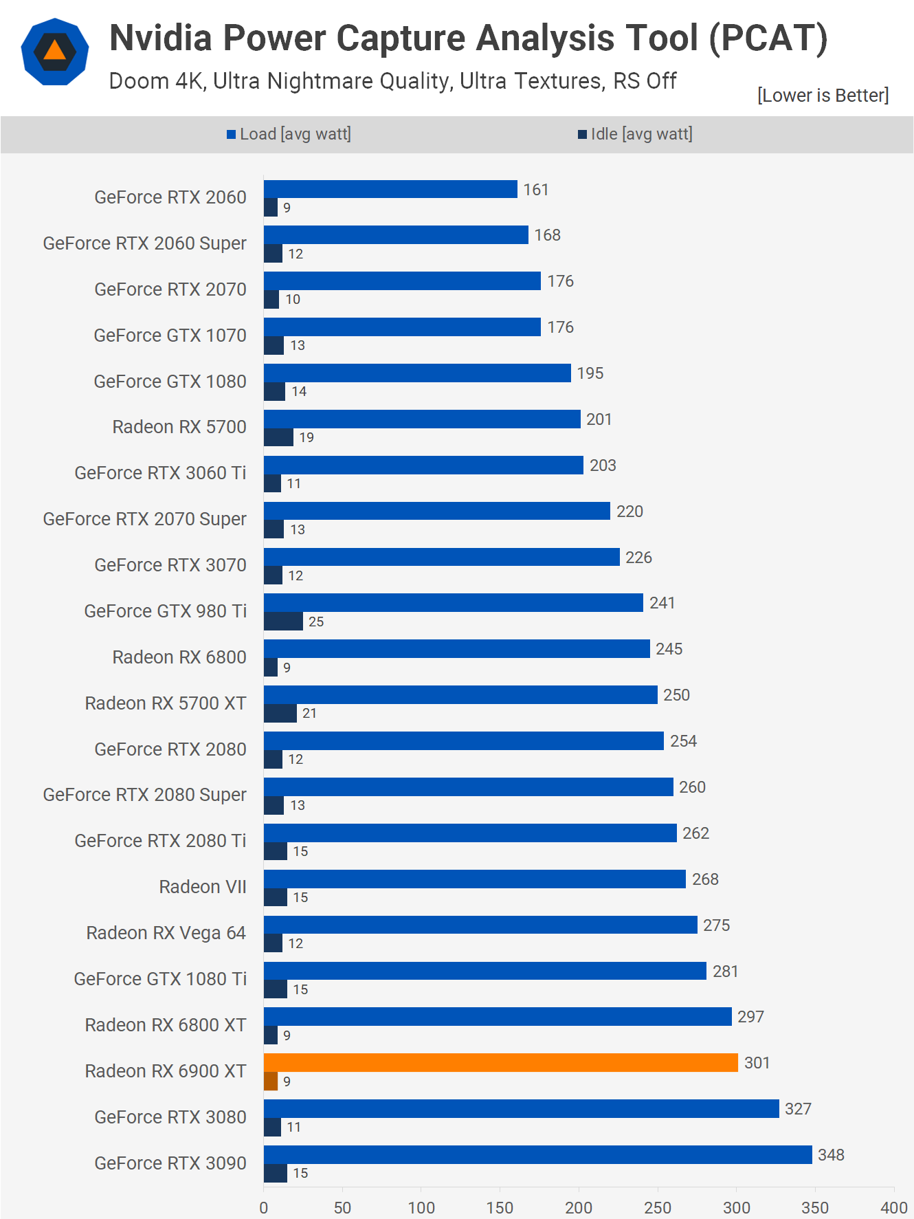
It's surprising to see them top the list of "Power per Watt", but I would have liked to have seen an "Energy Consumption" comparison.
 
It's surprising to see them top the list of "Power per Watt", but I would have liked to have seen an "Energy Consumption" comparison.
Here you go:

PCAT.png
 
Here you go:

Thanks. As expected, the Radeon is a power hog.

Pleasantly surprised to see a card as powerful as the RTX 2060 to also be the least power hungry. "Power consumption" is a major issue I consider when GPU shopping.
 
Radeon is great for winter time. The more you play, the warmer your apartment. So, if you're a teenager your parents will basically force you to play games all day long.
 
Back