Samsung's 4 nm process node achieves yield rates of 75 percent

nanoguy

Posts: 1,355   +27
Staff member
Why it matters: TSMC may be the current leader in process technologies, but Samsung is planning to take away its crown in the coming years. To that end, the Korean giant has already improved the yield rates on its 4 nm and 3 nm process nodes to the point where they could be considered commercially viable by companies like Nvidia, Qualcomm, AMD, and Google for their future chips.

Samsung's Foundry division has had a rough time holding onto customers over the past few years, mostly due to thermal and yield issues with its modern process nodes. These problems have convinced many including Nvidia and Qualcomm to go with TSMC for their current needs, but the Korean tech giant seems determined to repair its image as soon as possible and win back some contracts in the coming months.

According to Park Sang-wook, who is a researcher at Hi Investment & Securities, Samsung has managed to improve the yield of its 4 nm manufacturing node to around 75 percent. For reference, TSMC currently holds the crown in that department with yield rates approaching 80 percent. Last year, supply chain insiders noted Qualcomm Snapdragon 8 Gen 1 chips made using Samsung's 4 nm process node had yield rates of around 35 percent, which is why Qualcomm went to TSMC for the Snapdragon 8 Gen 2 SoC and Nvidia did the same for its RTX 40 series GPUs.

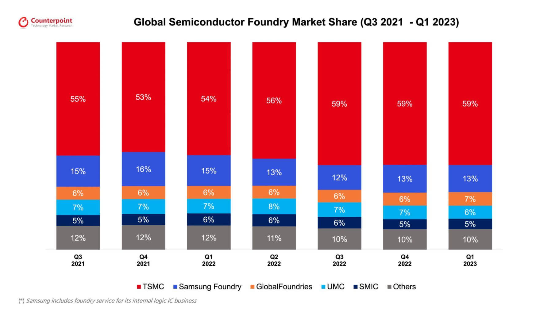
Interestingly, Sang-wook says that Samsung has also made great strides when it comes to its 3 nm process. Current yield rates hover around the 60 percent mark, which is already better than TSMC's equivalent node where 55 percent of the chips on a wafer are usable. This means the Korean company has a chance to convince some of its former customers to opt for its manufacturing services, though that will also depend on pricing for wafers made using the new node.

Now read: There is TSMC and there's everybody else, can Samsung or Intel catch up?

Given that TSMC's 3 nm capacity is almost completely booked by Apple, we might even see AMD CPUs and GPU chiplets manufactured by Samsung in the coming years. Google has also shown some interest in making Tensor G3 chips at Samsung's fabs, but we'll have to wait and see.

Meanwhile, Samsung's strategy is to focus on long-term efforts like building the world's largest chip center in South Korea using a gargantuan $230 billion investment fund. The facility won't become operational until 2042, however, which is ample time for Samsung to refine its process technologies. On that front, the company says it's on track to produce chips using 2 nm and 1.4 nm-class nodes in 2025 and 2027, respectively.

Masthead credit: Sebastian Moss

Permalink to story.

 
Few corrections.

- Nvidia used Samsung 8nm for GPUs, not 4nm. Nvidia went for Samsung because Nv*****s do not really care abou power consumption because of (useless) RT performance. Also going back for TSMC makes 4000 series look better.

- Apple has booked most of 3nm early production but AMD is only interested TSMC 3 nm much later. AMD just released TSMC 5nm products and will wait until real mass production begins
 
Kind of interesting how the human market and govt subsidies work - Trillions in subsidies and Investments in consumption -
then less than one year to make a numerous Covid 19 vaccines.

So wonder when the trillions will come ( a cheap cost ) to sort out as the nature global temp rises YOY for the next century plus - as Big energy , big money and right wing extremist declare - I mean man made or not - all the predictions are going up up and no down down - in fact Big Energy is struggling to find any sane scientists to sell it will soon come down - of the 100 scientists they championed in the last 2 decades - Not One Has Been Right - not one - they get dumped and for next solo genius fighting the brave fight


I believe that each IC design has its own yield rate (different area, different built in redundancy). Unless you have a comparable IC built on both processes it is hard to compare the percentage. I believe a better metric is defects/area or defects/million transistors.
 
Kind of interesting how the human market and govt subsidies work - Trillions in subsidies and Investments in consumption -
then less than one year to make a numerous Covid 19 vaccines.

So wonder when the trillions will come ( a cheap cost ) to sort out as the nature global temp rises YOY for the next century plus - as Big energy , big money and right wing extremist declare - I mean man made or not - all the predictions are going up up and no down down - in fact Big Energy is struggling to find any sane scientists to sell it will soon come down - of the 100 scientists they championed in the last 2 decades - Not One Has Been Right - not one - they get dumped and for next solo genius fighting the brave fight

Not sure how this is on subject...
 
Wow, those yields are still rather low. Traditionally I think the aim was to get at least 90% yields. Well, these fab processes are getting more and more complex (and more prone to error, some positioning error that would not even be a problem 5 years ago would wreck the whole wafer now) so I guess.
 
Just saying 'yield' means nothing.
They may have 25% with a defect, but how many of those can just have some cores deactivated? We all know where i3 and i5s come from.
 
Just saying 'yield' means nothing.
They may have 25% with a defect, but how many of those can just have some cores deactivated? We all know where i3 and i5s come from.
Indeed true. In the past, the most they had were things like the 486SX, originally a 486 with the math coprocessor fused off (so they could use chips where the defect was there rather than in the main CPU). And I think they sold 487 chips for that that were the opposite, a full 486 with the CPU fused off. Now, AMD has chiplets (less to throw out in case of a severe flaw) and both AMD and Intel sell models with some cores fused off (like the AMD hexacores, an 8-core with 1 core on each chiplet fused off.)
 
Indeed true. In the past, the most they had were things like the 486SX, originally a 486 with the math coprocessor fused off (so they could use chips where the defect was there rather than in the main CPU). And I think they sold 487 chips for that that were the opposite, a full 486 with the CPU fused off. Now, AMD has chiplets (less to throw out in case of a severe flaw) and both AMD and Intel sell models with some cores fused off (like the AMD hexacores, an 8-core with 1 core on each chiplet fused off.)
Actually 487's were fully functional 486's but designed to be inserted into the upgrade socket.

(Damn I'm old...)
 
Back