Analysts believe that a single TSMC 5nm wafer costs $17,000

mongeese

Posts: 643   +123
Staff
In brief: CSET (The Center for Security and Emerging Technologies) has published a new report, titled “AI chips: What they are and why they matter,” in which they calculate the sales price of silicon wafers. They found that TSMC’s 5nm node requires exceptionally expensive wafers that aren’t cheaper on a per-chip basis than 7nm chips. However, they still believe that 5nm chips are a popular purchase.
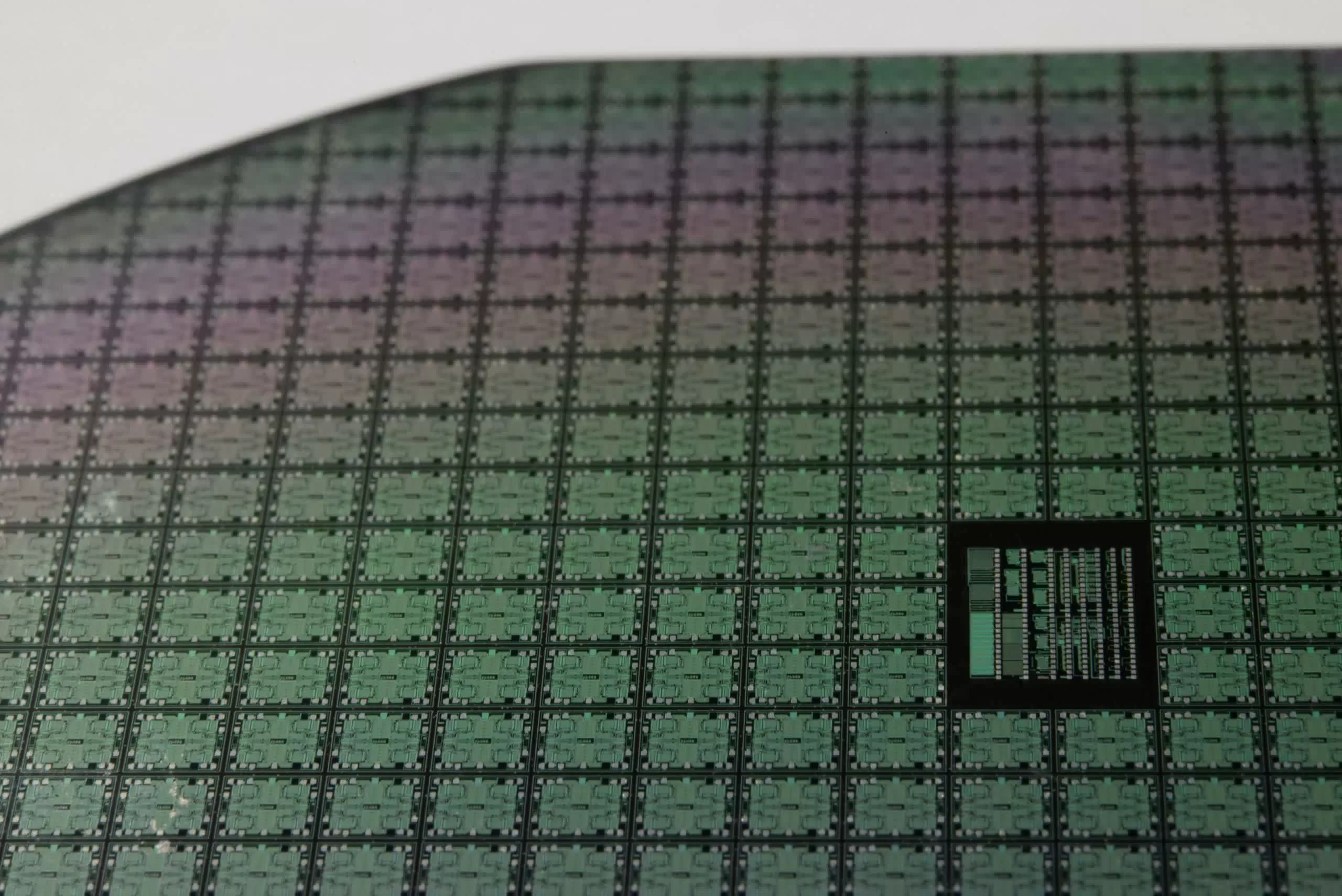
According to CSET’s model, a single 300 mm wafer built on the 5nm node costs approximately $16,988. A similar wafer built on the 7nm node reportedly costs $9,346.

Using a theoretical ~600 mm2 die, approximately equal in size to the Nvidia GA102 GPU used inside the RTX 3080 and RTX 3090, the per-chip costs of each die were calculated to be $233 and $238, for the 7nm and 5nm nodes, respectively.

CSET: Calculation of foundry sale price per chip in 2020 by node

  16/12nm 10nm 7nm 5nm
Mass production year and quarter 2015 Q3 2017 Q2 2018 Q3 2020 Q
Capital investment per wafer processed per year $11,220 $13,169 $14,267 $16,746
Capital consumed per wafer processed in 2020 $993 $1,494 $2,330 $4,235
Other costs and markup per wafer $2,990 $4,498 $7,016 $12,753
Foundry sale price per wafer $3,984 $5,992 $9,346 $16,988
Foundry sale price per chip $331 $274 $233 $238

The foundry sale price per wafer is calculated as the sum of the "other costs and mark-up per wafer" and the "capital consumed per wafer processed in 2020," or in other words, the sum of the profit margins, assembly cost, and estimated development cost. Consequently, this is an average value for only a small window of time; TSMC will be varying the actual sales price above and below this value depending on long-term strategies and market conditions.

Nevertheless, this is a rigorously estimated value and a good baseline for the actual sales price of the wafers. From it, we can deduce that 5nm products, including the processors used in the next generation of Apple handsets, will not be cheaper than existing products.

The high costs of 5nm production are largely a consequence of their novelty, and in time, they’ll become cheaper. However, the 5nm node does require some unique treatments that make it more expensive than older nodes. It is heavily reliant on EUV (extreme ultraviolet lithography) techniques, and reportedly, each EUV tool costs $120 million. A single wafer can have up to fourteen EUV layers applied to it.

Despite the cost, the 5nm node is a promising one. At the same power consumption as a 7nm chip, a 5nm one will run 15% faster. At the same performance level, a 5nm chip will consume 30% less power than a 7nm one. And the 5nm node is reported to have better yield rates, too.

Image credit: Laura Ockel

Permalink to story.

 
I'll probably buy a new console when their SoC make it onto 5nm. In a couple years at least. Both have huge cases, with highly strung hot running chips and industrial cooling solutions by the looks of them.

5nm will be just the ticket for their first hardware refresh. 30 percent less power consumption and thermals. But it'll be a while before the price is right for them, as the article makes clear.
 
I'll be coming back as my reincarnated self before I will be able to afford that baby ..... hopefully as a banker .... LOL
 
It looks like the node has a much better return for mobile parts. While a 15% performance increase is nothing to scoff at, 30% less power at the same performance sounds even better.

Quick question: Are the values given for 5nm EUV vs. 7 nm EUV or 7nm non-EUV ?
 
It looks like the node has a much better return for mobile parts. While a 15% performance increase is nothing to scoff at, 30% less power at the same performance sounds even better.

Quick question: Are the values given for 5nm EUV vs. 7 nm EUV or 7nm non-EUV ?
Looks like the normal N7 process
https://www.tsmc.com/english/dedicatedFoundry/technology/5nm.htm
But as you can see the same process sees improvement overtime and for which devices would better benefit the truth both mobile and high performance will benefit but because of chips size, yield and sequentially costs mobile devices will usually the first to utilize it. How high performance would utilize better consumption is fairly easy - while mobile devices are more thermally constrained also high performance devices are and the combination of better transistor density with lower power can allow more advanced design to be utilized and have better performance without changing the frequency (which is the metric of performance that is usually referred).
density is always a critical metric because how complex or scaled a design can be usually depends on how many transistor you have available and there is a limit for the reticle size of the mask which if I'm correct may produce chips up to 858 mm^2, but even if you don't build such large chip there are always benefits for having smaller chip.
 
It looks like the node has a much better return for mobile parts. While a 15% performance increase is nothing to scoff at, 30% less power at the same performance sounds even better.
It's a shame that it's never both the newer node - performance increase for the same power consumption or lower power consumption for the same performance. Imagine the chips if one could have with 15% more speed for 30% less juice :)
 
It's a shame that it's never both...
Well of course the power-performance graph is a curve, not a binary choice. TSMC quotes both ends of the curve, but for any given part, a customer can choose other points along it.
 
I'll probably buy a new console when their SoC make it onto 5nm. In a couple years at least. Both have huge cases, with highly strung hot running chips and industrial cooling solutions by the looks of them.

5nm will be just the ticket for their first hardware refresh. 30 percent less power consumption and thermals. But it'll be a while before the price is right for them, as the article makes clear.
You will be waiting forever then, unless you opt for a Nintendo product which you can do even now.

Sony and MS will not reduce the size of console or power consumption at the cost of performance as the prime consideration for them is to build a system which will live on for five years. However, they get outpaced by latest hardware even before they are physically available.
They don't have any ground to give as then the disparity between PC and consoles will he so huge that people will no longer be excited about console games.
 
It's a shame that it's never both the newer node - performance increase for the same power consumption or lower power consumption for the same performance. Imagine the chips if one could have with 15% more speed for 30% less juice :)
Those days are over unfortunately. The industry needs a huge shift in technology before we see such gains again and I don't see that happening in the next 5-6 years. We'll eventually get to 2nm and then stick with it for a while.
 
Those days are over unfortunately. The industry needs a huge shift in technology before we see such gains again and I don't see that happening in the next 5-6 years. We'll eventually get to 2nm and then stick with it for a while.
Nevermind controlling electron tunneling in any sub-2nm processor, I'm pretty sure that you would have to switch to something more exotic than photons to make those processors - which will be much harder to focus in any meaningful way.

My bet is that 2-3nm is a hard wall for silicon processors as we known them.
 
My bet is that 2-3nm is a hard wall for silicon processors as we known them.
Quite likely ... but remember that what the industry will call the 3nm node will likely have feature sizes around three times that. The node names have been marketing than descriptive for several years now. So we're more than 5 years away from that hard wall.
 
Quite likely ... but remember that what the industry will call the 3nm node will likely have feature sizes around three times that. The node names have been marketing than descriptive for several years now. So we're more than 5 years away from that hard wall.
I meant 'literal 3nm'. I don't see photon-based lithography working beyond that, and focusing other particles or waves with any kind of precision gets much more difficult.
 
I meant 'literal 3nm'. I don't see photon-based lithography working beyond that, and focusing other particles or waves with any kind of precision gets much more difficult.

You can't get anything smaller than a photon, you just need to increase its frequency if you want to decrease the feature size. A gamma ray is still a photon.
 
You can't get anything smaller than a photon, you just need to increase its frequency if you want to decrease the feature size. A gamma ray is still a photon.
E=hf. The higher the frequency, the higher the energy ... and the higher the energy, the more damage the particle does when it strikes. Even at EUV frequencies, erosion and ionization of the target is a problem, and ionization effects cause chemical changes in the silicon as well.
 
You can't get anything smaller than a photon, you just need to increase its frequency if you want to decrease the feature size. A gamma ray is still a photon.
The operative word is "focus" here. We already struggle to focus very high frequencies of UV light, and you think we could do it with a gamma ray just because it is a photon? If you have a way to do it, you should patent it and then go license it to all the fabs, because you'd become a very rich man practically overnight.
 
Back