Leaked slides detail Intel's 2013 Haswell architecture

Matthew DeCarlo

Posts: 5,271   +104
Staff

We're still roughly five months away from Sandy Bridge's die shrink, Ivy Bridge, but Intel is already preaching the virtues of its 2013 microprocessor technology. Codenamed Haswell, the architecture was first announced during September's IDF with limited info, but freshly leaked slides have revealed further details. We already knew that Haswell would use the same 22nm fabrication process and 3D tri-gate transistors as Ivy Bridge to create an ultra-efficient package that reduces platform power by a factor of 20 without sacrificing performance.

intel haswell

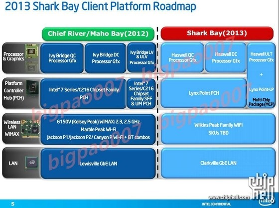
Based on the latest information, Haswell will be a part of a platform dubbed "Shark Bay" and the chips will require entirely new motherboards -- desktop versions will interface via LGA-1150 while mobile iterations will use either rPGA947 or BGA1364. Desktop Haswell parts will carry two or four processing cores alongside an on-die graphics chip that supports DirectX 11. They'll also support Intel's Hyper-Threading and Turbo Boost technologies as well as the AVX 2.0 instruction set, dual-channel DDR3 1600MHz RAM and PCI Express 3.0.

intel haswell

Haswell will come in various power brackets. Desktop chips will have a TDP of 35W and 95W, mobile variants will come in 37W, 47W and 57W TDPs, and low-voltage parts for ultrabooks will sip only 15W. This is expected to grant notebooks with "all-day" battery life. Back at IDF, Intel demoed a chip that was being powered by a single UV light pointed at a solar cell the size of a postage stamp. That efficiency will be further amplified in 2014 when Intel ships the 14nm die shrink of Haswell called Broadwell, but virtually no details are available on that yet.

Permalink to story.

 
"the chips will require entirely new motherboards"

Intel and super duper new chip!! Surprise Fn Surprise Fn Surprise.

1155, 1156,1366 for i7 series

1155, 1156 for i5 and i3 series.

not all chipsets support all CPUs in series. Revisions changing the rules sprinkled through the CPU lifetime. Whatever the benefits of the 'New Latest Greatest' (or is that Gratest as in to grate as on one's nerves?) is it worth the constantly changing landscape of motherboard chipsets and uncertain upgrade paths?

Here we go again with yet another iteration from Mount Intel. I keep expecting to see Rambus resurrected one of these days.
 
Why can't intel just use the same sockets in a different chipset? I understand the reason for a chipset change, but not so much on the socket.
 
Why can't intel just use the same sockets in a different chipset? I understand the reason for a chipset change, but not so much on the socket.
What would be the point ? How would you use an Ivy Bridge or Sandy Bridge CPU on a motherboard whose CPU voltage regulation has been removed because it is now part of the Haswell CPU ? (See this article from three days ago )
On the integration front, there are system level enhancements that would help board and system designers get things done faster and better, and should I say cheaper...the voltage regulators are to be fully integrated in the CPU, greatly assisting the power design, not just the overclockers.

Haswell schematic

From the VR-Zone article:
What the slides do give away is that Intel has at least made one major change to the Shark Bay platform, there's no longer an FDI interface, which is used for piping the display connectivity via the PCH on the 6 and 7-series chipsets
Hence the decreased pin count of the socket. Haswell is simply continuing Intel's design philosophy of moving all functionality to the CPU package - what started with an integrated memory controller is now moving closer to a system on a chip (SoC)

Socket change makes no sense. but whatev.
See above...unless you're just trolling, in which case go for gold.
 
Do you think this is standard PR or have they solved signaling down to 10-14nm yet?
I am assuming that tri-gate has good deal to do with this if so.
 
Win7Dev said:
Why can't intel just use the same sockets in a different chipset? I understand the reason for a chipset change, but not so much on the socket.

AMD tried that, you see where it got them!
 
mount intel needs to make more money with every new chip they put out. can't blame them since that's the way they want to do things in a company's perspective. who wouldn't want to make more bucks from their brain? It's not mother Teressa orphanage it's freaking intel!
 
Do you think this is standard PR or have they solved signaling down to 10-14nm yet?
I am assuming that tri-gate has good deal to do with this if so.

That I'm not sure of. What is known is that 22nm (and presumeably tri-gate transistors) works, since Intel already have working silicon of Haswell.
As far as I'm aware 14nm (Broadwell) is still set for double-pattening immersion lithography- so should be a known quantity. As far as 10nm is concerned that requires EUV to be viable. Intel are already on record as saying that their cadence might slip due to tooling not being ready. From what I gather EUV seems to be making steady progress, and Intel have already signed up for ASML's next-gen NXE:3300 lithography tool...so assuming that ASML get the throughput ironed out, and more importantly a viable metrology tool for inspecting EUV masks for defects eventuates then it becomes a matter of waiting for each branch of the process to blend into a viable process ( microarchiture, EUV tools, calibration and QC)...how critical the timing is probably depends on the what kind of manufacturer competition factors are in play in 2018 or so.

As far as I'm aware signalling on what Intel have planned should be viable down to 10-12 x the thickness of the silicon atom -which should be ~5-6nm

/man, thats a sh$@load of links!

EDIT: Sub-10nm finFET process discussed here pdf. I think we covered some of this in an earlier thread (ostensively about Bulldozer I believe) between me, Archean and yourself.
 
@supersmashbrada: I can't tell if you're joking or not. AMD being the underdog has absolutely no relation to them choosing to keep supporting current sockets.
 
Guest said:
@supersmashbrada: I can't tell if you're joking or not. AMD being the underdog has absolutely no relation to them choosing to keep supporting current sockets.

You completely missed the point. Who said anything about supporting current sockets. What current socket? How old is AM3? Riddle me this batman...riddle me this.
 
supersmashbrada said:
Win7Dev said:
Why can't intel just use the same sockets in a different chipset? I understand the reason for a chipset change, but not so much on the socket.

AMD tried that, you see where it got them!

Sales?

I'm sure AMD got quite a few sales thanks to the compatibility. Without it Intel might have have had even more market share. At most points in time in the past couple of years Intel was a more attractive choice for a new PC, but if you need more processing power and can just upgrade the CPU without having to buy other upgrades that often trumps the advantages of the competition. I'm running a Phenom II X6 on an AM2+ board and I'm quite happy with that.
 
The ONLY reason AMD carries over sockets is because their weren't enough architectural changes to the die to warrant a new socket. Not to mention, their chipsets haven't been anything to get excited over either. Trust me, if AMD wasn't in the rough, the tables would quickly turn. AMD is not keeping up this socket compatibility for your benefit. If you believe that, then god help us all.
 
PCH is going onto the CPU die. Not much left... can wifi fit inside a cpu die? lol
Yes.
And I/O (southbridge) as well as on-die stacked RAM integration probably isn't that far away.

Sales? I'm sure AMD got quite a few sales thanks to the compatibility
No doubt. But that was then, this is now. Very few people I know went with Bulldozer and opted to use an 890/870 chipset board.
Compatibility is largely a myth now in any case. AMD's 45nm line is now on death row, and BD- whilst not requiring a new socket, does require a new motherboard. Socket FM1 is a one-hit wonder likely to have a shorter lifespan than any Intel socket in commercial use...assuming AMD's Trinity timetable is to be believed - and that, based on AMD's less than accurate portrayal of Bulldozer is by no mean a given
Without it Intel might have have had even more market share. At most points in time in the past couple of years Intel was a more attractive choice for a new PC, but if you need more processing power and can just upgrade the CPU without having to buy other upgrades that often trumps the advantages of the competition.
Looking backward doesn't stop you tripping over what's sitting in front of you though does it? Expecting AMD to keep putting R&D into Athlon II/Phenom II and keeping that compatibility/upgrade path open ? Where's the upgrade path for people that bought into an FM1/Llano system ?
The forums are awash with people who bought into 990FX/990X/970 chipset motherboards solely on the strength of AMD's promised BD performance, can you categorically say that AMD and motherboard vendors wont pull the same stunt again with Piledriver, Steamroller and Excavator ?
I'm running a Phenom II X6 on an AM2+ board and I'm quite happy with that.
I'm sure with customers who think like yourself, it's only a matter of time before AMD's sales pick up I guess.
 
Do you think this is standard PR or have they solved signaling down to 10-14nm yet?
I am assuming that tri-gate has good deal to do with this if so.

That I'm not sure of. What is known is that 22nm (and presumeably tri-gate transistors) works, since Intel already have working silicon of Haswell.
As far as I'm aware 14nm (Broadwell) is still set for double-pattening immersion lithography- so should be a known quantity. As far as 10nm is concerned that requires EUV to be viable. Intel are already on record as saying that their cadence might slip due to tooling not being ready. From what I gather EUV seems to be making steady progress, and Intel have already signed up for ASML's next-gen NXE:3300 lithography tool...so assuming that ASML get the throughput ironed out, and more importantly a viable metrology tool for inspecting EUV masks for defects eventuates then it becomes a matter of waiting for each branch of the process to blend into a viable process ( microarchiture, EUV tools, calibration and QC)...how critical the timing is probably depends on the what kind of manufacturer competition factors are in play in 2018 or so.
As far as I'm aware signalling on what Intel have planned should be viable down to 10-12 x the thickness of the silicon atom -which should be ~5-6nm
Took a while, but it looks like ASML and Intel are finally moving apace with EUV tooling...has it been eight months already?
 
Back