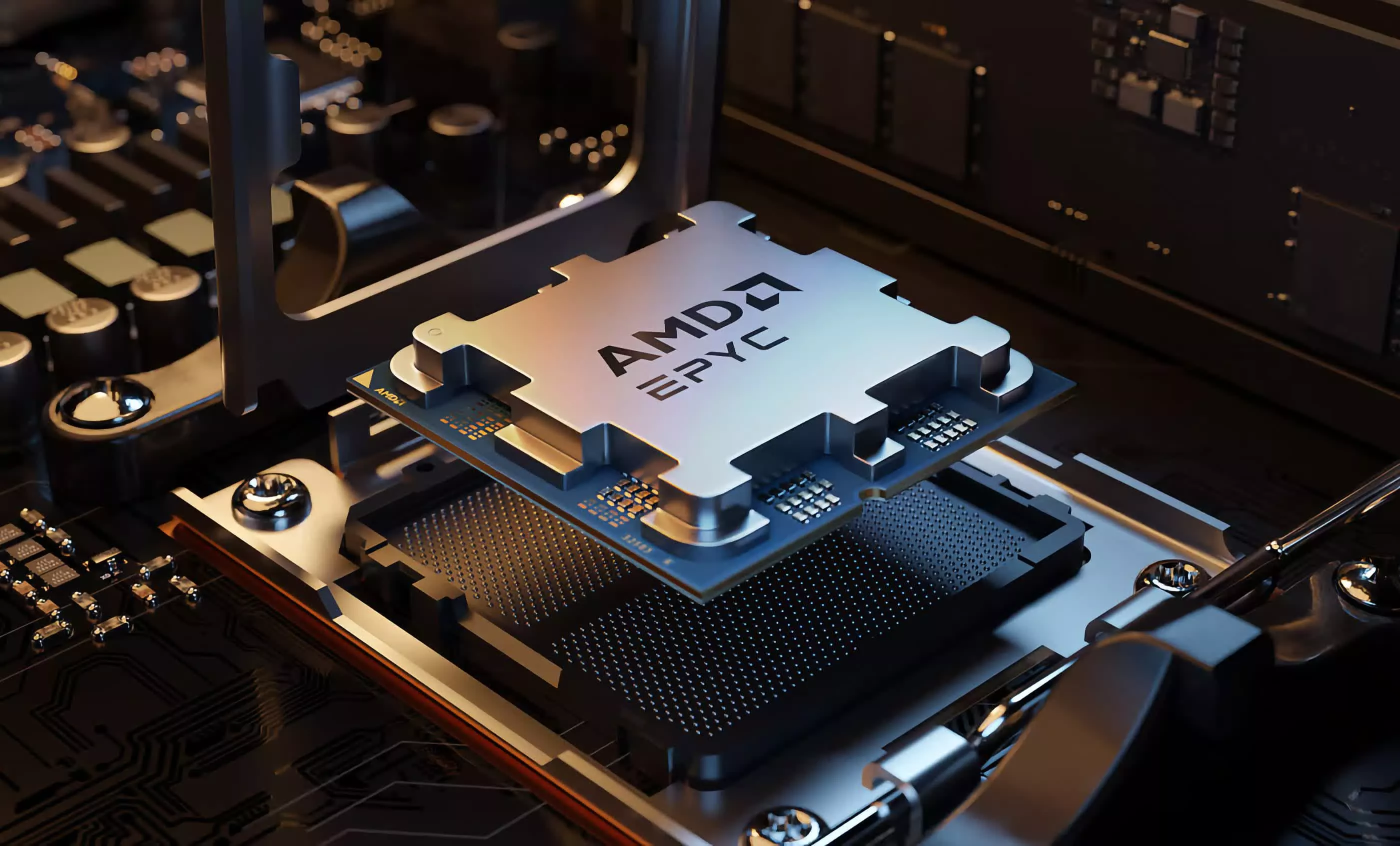
First look: AMD's next-generation Epyc Venice server chip has begun its production ramp on TSMC's N2 node, the foundry's new 2nm-class process. That move brings a 256-core server part onto one of the most advanced nodes at a time when data centers are straining to add capacity for AI and other agentic workloads.
Venice is a 6th-gen Epyc chip based on the Zen 6 core architecture and targeted at dense data center workloads. AMD is claiming more than a 70% improvement in overall performance and efficiency versus the current Epyc Turin chips, along with more than a 30% increase in thread density.
The extra performance is not just from adding cores; AMD is also leaning on IPC improvements, higher clocks, and changes in the core and uncore design to close the gap. The lineup is expected to include a 96-core part and a much denser 256-core, 512-thread model, lifting the top core count by about one-third over Turin's 192-core, 384-thread ceiling.
The Venice platform is designed to keep those cores and any attached accelerators supplied with data. Its new SP7 socket exposes up to 16 memory channels per socket, for roughly 1.6 TB/s of aggregate memory bandwidth.
AMD also says Venice doubles CPU-to-GPU bandwidth over today's platform, which almost certainly comes from adding PCIe 6.0 and its higher per-lane throughput.
At the silicon level, Venice is built on TSMC's N2 process, which switches from FinFETs to nanosheet gate-all-around transistors. TSMC says N2 offers about 10 – 15% higher performance at the same power, or 25 – 30% lower power at the same performance, compared with N3E, along with up to 15% more transistor density.
In practice, that lets AMD either add more cores, cache, and I/O within the same power envelope or keep performance flat while cutting power per socket. Both options matter for operators trying to increase AI capacity without blowing through power and cooling limits.

TSMC started N2 volume production late last year and is ramping multiple fabs on the node to handle demand. Apple is widely reported to have locked up most of the early N2 capacity for consumer chips, but Venice is the first high-performance compute part publicly announced as entering a production ramp on the node.
Because server dies are far larger and more complex than phone SoCs, qualifying a 256-core Epyc on N2 suggests the node is ready for big AI and cloud chips. AMD also intends to produce Venice at TSMC's Arizona site once its 2nm lines are running, giving the chip a US manufacturing base.
AMD has also confirmed Verano, another sixth-generation Epyc part on the same 2nm node, positioned around performance-per-dollar-per-watt. The company describes it as an AI-focused spin on Venice, tuned for agentic AI workloads. It adds newer memory standards, including LPDDR, to drive more bandwidth and better efficiency in dense AI racks.