WTF?! Building semiconductors usually requires billion-dollar fabs, stadium-sized cleanrooms, and equipment that costs more than most homes. But that didn't stop one YouTube channel from attempting something much smaller: a Class 100 semiconductor cleanroom built inside a backyard shed.
The YouTube channel, appropriately named Dr. Semiconductor, recently posted a video showing off the DIY lab, which was built to handle at least some of the early processes involved in chipmaking.
While nobody is about to start mass-producing rival GPUs to challenge Nvidia from a garden outbuilding, the project is still an impressive demonstration of how far determined enthusiasts can go with enough planning, engineering knowledge, and filtration.
Modern semiconductors are manufactured in ultra-clean environments because even a tiny dust particle can ruin a wafer. Commercial fabs from companies like Intel, Samsung, and TSMC spend vast sums creating controlled spaces that are thousands of times cleaner than a hospital operating room.
Dr. Semiconductor's version is obviously a little more modest, but the principles are the same.
What began as an ordinary wooden shed was converted into a controlled lab space with insulation, framing for cleanroom-grade HEPA filters, dedicated electrical systems, and a mini-split HVAC setup.
The interior was divided into two zones: a gowning area and the cleanroom itself. Instead of expensive industrial paneling, the builder used flame-resistant drywall coated with water-based epoxy to create a smooth, cleanable surface.
The key is airflow. Filtered air is pushed downward in laminar flow while the room is kept at positive pressure, helping prevent contaminated outside air from entering.
After borrowing a particle counter to verify the results, Dr. Semiconductor recorded around 40 particles per cubic foot, with edge measurements staying under 100. That puts the space in the Class 100 cleanroom category, at least in terms of particle count.
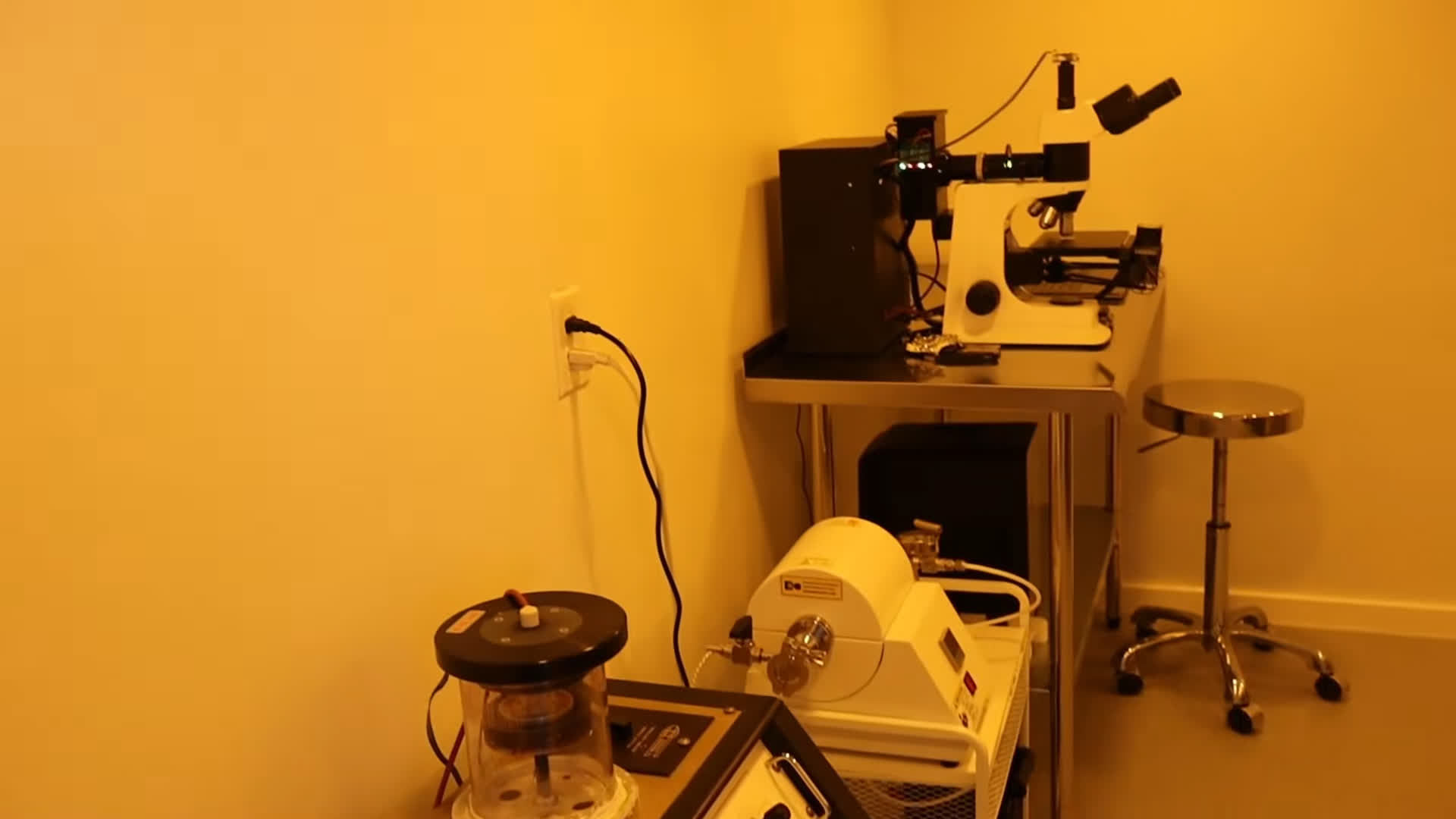
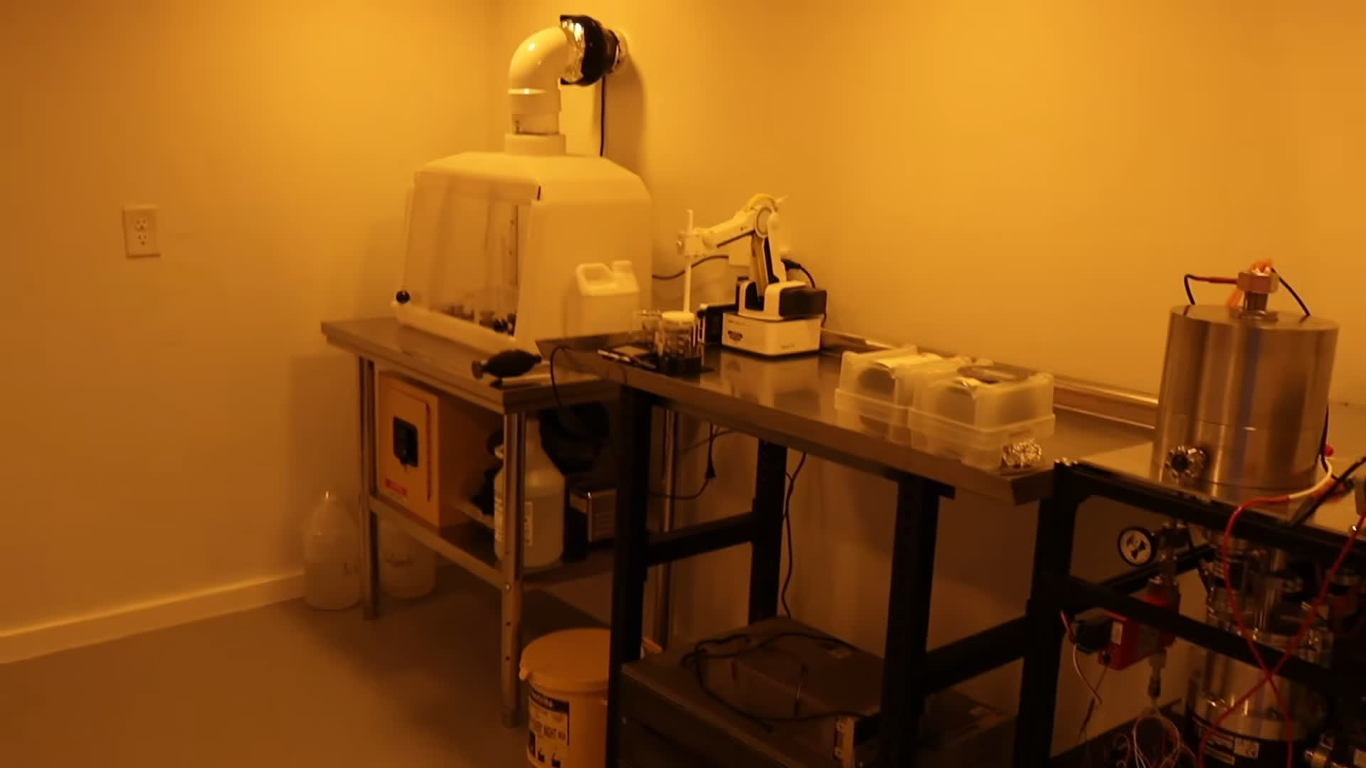
The shed doesn't just contain clean air, either. The lab also includes a plasma etcher, a vacuum furnace for annealing, a fume hood for chemical processing, a 3D-printed spin coater, a robot arm for automated cleaning, and a thin-film deposition system.
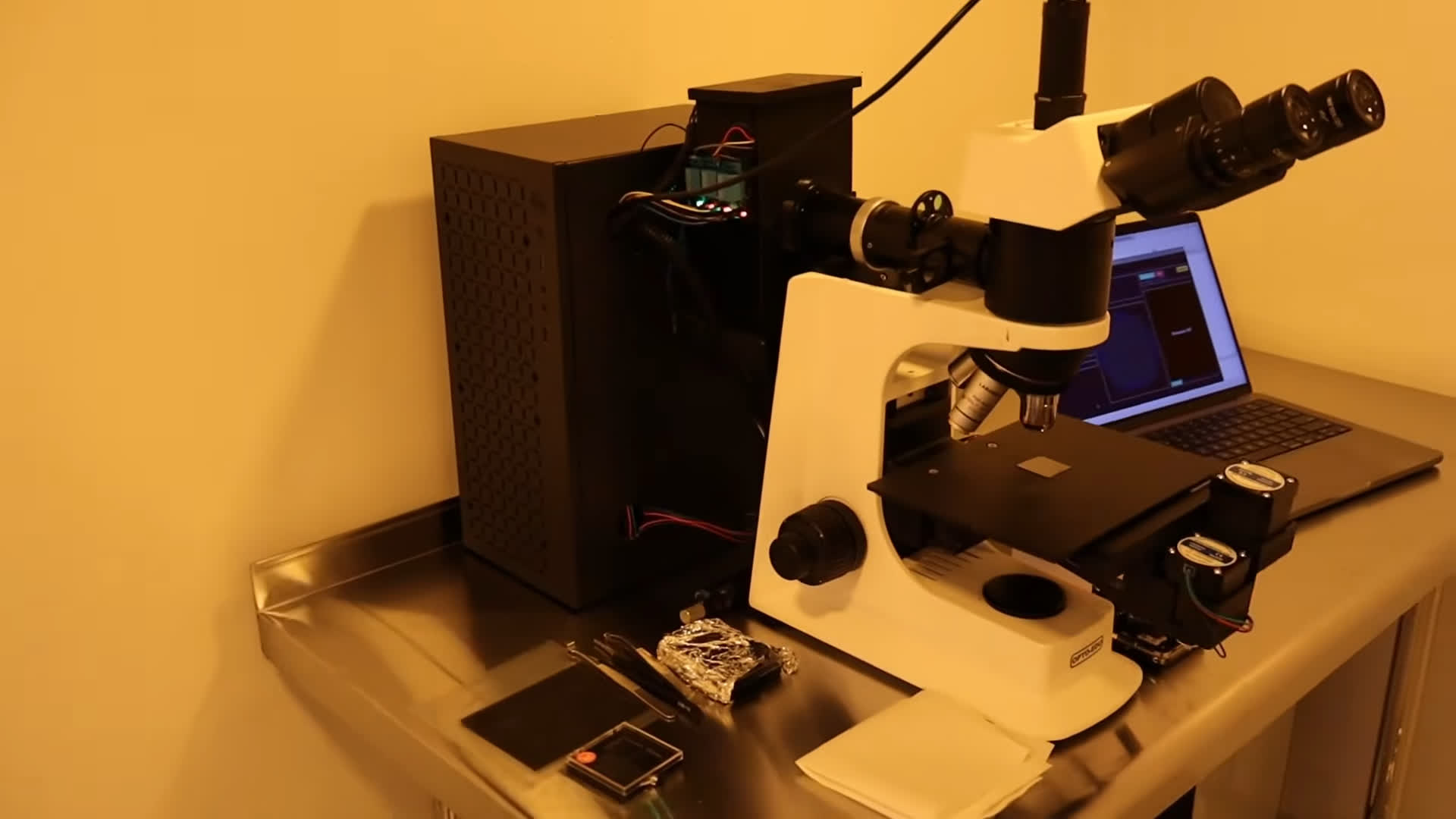
Propably the most notable item is a custom lithography machine based on a microscope and controlled through custom software, which the creator says is capable of submicron patterning.
That doesn't mean backyard chip fabs are suddenly practical. As others have pointed out, building a cleanroom is only one part of an incredibly expensive and complex process. Producing modern CPUs or GPUs still requires a staggering amount of specialized hardware, software, and intellectual property.