
The takeaway: The race toward sixth-generation wireless communications took a decisive step forward this month as researchers in Singapore, France, and the United States unveiled a compact terahertz antenna built on principles borrowed from topological photonics. The team, led by Ranjan Singh of the University of Notre Dame, created a silicon-based design capable of managing high-frequency, information-rich signals without relying on complex mechanical components.
The breakthrough, detailed in Nature Photonics, centers on a fundamental problem facing 6G: how to efficiently transmit and receive data at terahertz frequencies. These frequencies, which are thousands of gigahertz above current 5G bands, can carry staggering amounts of information, theoretically approaching one terabit per second.
That throughput could move half the content of a modern smartphone in under a second. Yet the same high frequency that unlocks this performance also makes antenna design extraordinarily difficult. Signal losses increase, directionality becomes unstable, and even minor structural imperfections can scatter waves.
Instead of scaling up traditional antenna arrays or adding moving beam-steering elements, Singh and his team approached the problem from a photonics angle. Topological photonics, a relatively young discipline, explores how light – or more generally, electromagnetic waves – can be forced along predetermined paths that remain stable even when the underlying material is imperfect or irregular. By carefully arranging geometric features in a material, scientists can create "protected" modes for light, akin to setting unbreakable rail tracks for photons.
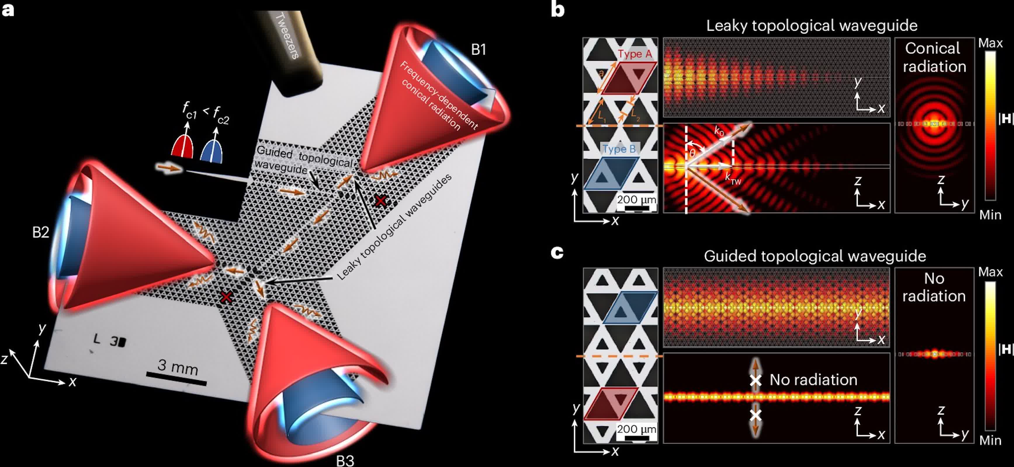
In the team's prototype, the medium is a precisely engineered silicon chip perforated with an intricate honeycomb of triangular holes. The holes occur in two distinct sizes – 99 micrometers and 264 micrometers across – and their placement dictates how terahertz radiation behaves inside the material.
When a specific pattern of the two hole sizes is printed, the light confinement changes; electromagnetic waves can either remain guided within the chip or intentionally "leak" outward at an angle. This controlled leakage forms a conical beam of terahertz radiation, transforming the patterned chip into a compact, passive antenna.
Experiments showed that this geometry-based control enables the device to radiate across roughly three-quarters of the surrounding spatial volume. That 75% coverage surpasses most existing terahertz antennas by a factor of 30.
The receiver collects inbound THz signals over a similarly broad field of view. Through these tests, the research group recorded data transmission rates hundreds of times faster than comparable state-of-the-art devices.
Crucially, the antenna accomplishes all of this without moving components or active beam steering. The control resides entirely in its physical design – the patterned topology that governs how electromagnetic energy propagates.
Looking ahead, Singh's group plans to integrate additional system functions directly onto the same silicon platform. The goal is to merge transmission, reception, and on-chip signal processing into a unified terahertz communication module. If successful, such integration would condense the entire front end of a 6G network device into a single miniature chip – an advance that could bring terahertz communication out of the laboratory and into commercial viability.