Serving tech enthusiasts for over 25 years. TechSpot means tech analysis and advice you can trust.
When you buy through our links, we may earn a commission.
The CPU is often called the brains of a computer, and just like the human brain, it consists of several parts that work together to process information. Some take information in, some store it, some process it, and others send the results back out. In today's explainer, we'll go over the key elements that make up a CPU and how they all work together to power your computer.
This article is part of our Anatomy series, which dissects the tech behind every major PC component. If you want to go even deeper, our CPU Design series covers how processors are designed and built in much more technical detail. This article goes over some of those fundamentals at a higher level and brings them up to date with how modern CPUs actually work.
Compared to other articles in our Anatomy series (see the full list of hardware components below), this one will inevitably be more abstract.
When you're looking inside something like a power supply, you can clearly see the capacitors, transformers, and other components. That's simply not possible with a modern CPU since everything is so tiny and because chipmakers like Intel, AMD, Apple and Qualcomm only share their designs at a high level. The actual circuitry is proprietary, so the topics covered in this article represent the general features that all CPUs have.
You might have a PC at work or at home. Maybe you use it to file tax returns, play the latest games, or even build and customize your own system. But how well do you really know the components that make up a PC?
It's also worth noting that what we call a "CPU" today is rarely just a CPU. Most modern processors are closer to a system-on-a-chip, packing integrated graphics, AI accelerators, memory controllers and more alongside the CPU cores.
It's also worth noting that what we call a "CPU" today is rarely just a CPU.
Every digital system needs some form of a Central Processing Unit. Fundamentally, a programmer writes code to do whatever their task is, and then a CPU executes that code to produce the intended result. The CPU is also connected to other parts of a system like memory and I/O to help keep it fed with the relevant data. Let's dive in...
The CPU Blueprint
When analyzing any CPU, the first thing you'll come across is the Instruction Set Architecture or ISA. This is the figurative blueprint for what a CPU can do and how software communicates with it. Just like there are many breeds of dogs within the same species, there are many different types of ISAs a CPU can be built on.
The two most common types are x86, which is most dominant in desktop PCs, laptops and servers, and Arm, which powers nearly every smartphone and has spread well beyond mobile. Apple moved the Mac to its own Arm chips in 2020, Qualcomm's Snapdragon X processors brought Arm to Windows, and Arm designs now run a growing share of cloud and AI server chips from Amazon, Nvidia and Google.
There are others too. RISC-V, an open and royalty-free ISA, has grown from a niche project into a serious contender. Billions of RISC-V cores already ship inside microcontrollers and the architecture is slowly pushing into PCs, servers and AI chips. Older ISAs like MIPS and PowerPC have faded into niche roles.
An ISA specifies what instructions the CPU can process, which registers software can use, how memory is addressed, and more.
How a chip actually carries out those instructions, including its pipeline, caches and execution units, is called the microarchitecture, and that's where chipmakers compete.
AMD's Zen 5 and Intel's Lion Cove cores both run the same x86 code, but they are built very differently inside. ISAs also keep evolving: Intel and AMD formed an x86 Ecosystem Advisory Group in 2024 to coordinate future extensions to the architecture.
To cover the main portions of a CPU, we'll follow the path an instruction takes as it is executed. Different types of instructions may follow different paths and use different parts of a CPU, but we'll generalize here to cover the biggest parts.
We'll start with the most basic design of a single-core processor and gradually add complexity as we get towards a more modern design.
Control Unit and Datapath
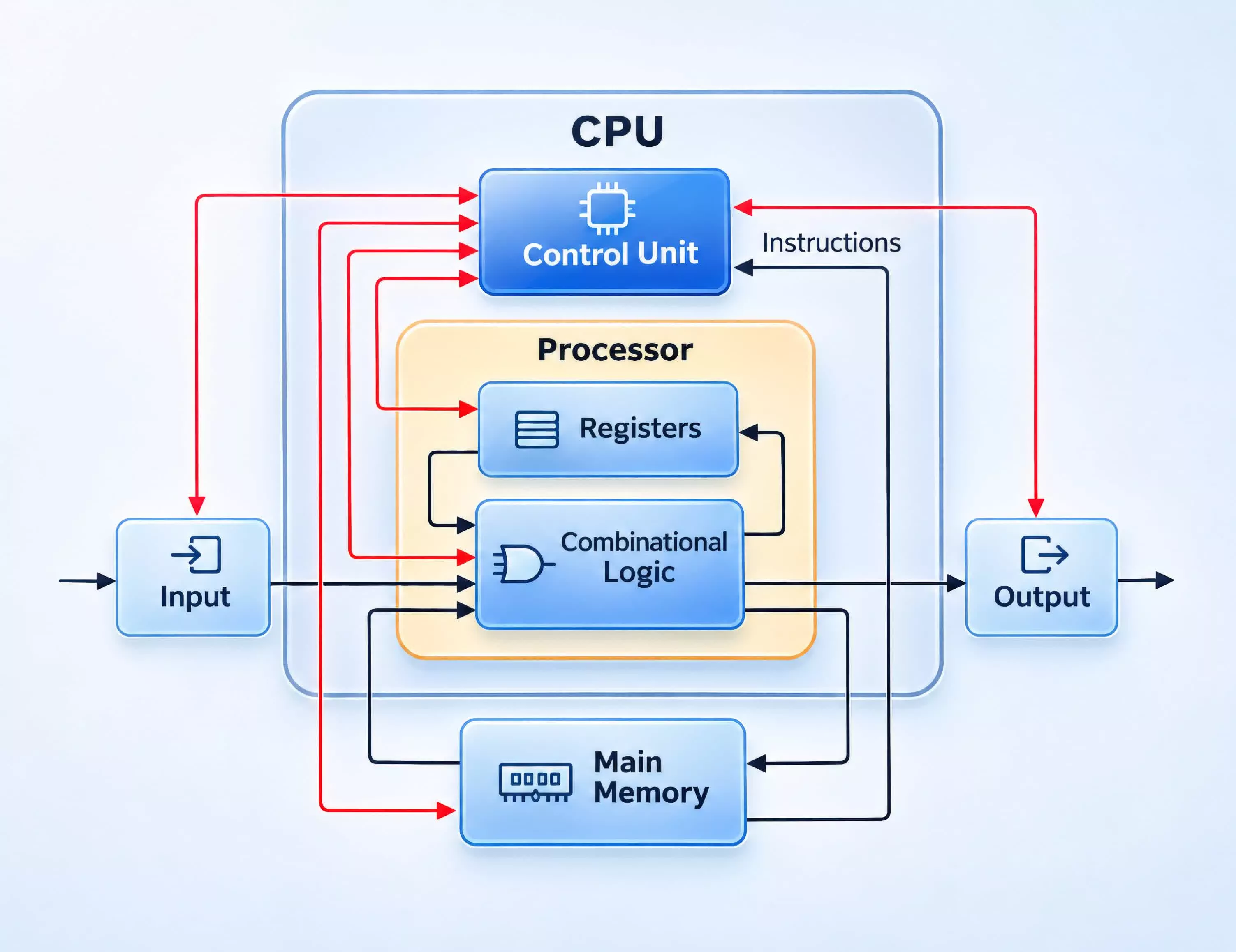
Block diagram of a basic CPU. Black lines indicate data flow, red lines indicate control flow.
The parts of a CPU can be divided into two: the control unit and the datapath. Imagine a train. The engine is what moves the train, but the engineer is pulling the levers behind the scenes and controlling the different aspects of the engine. A CPU is the same way.
The datapath is like the engine and, as the name suggests, is the path where the data flows as it is processed. The datapath receives the inputs, processes them, and sends them out to the right place when they are done. The control unit tells the datapath how to operate, like the engineer driving the train. Depending on the instruction, the control unit will route signals to different components, turn on and off different parts of the datapath, and monitor the state of the CPU.
The Instruction Cycle: Fetch
The first thing our CPU must do is figure out what instructions to execute next and transfer them from memory into the CPU. Instructions are typically produced by a compiler and are specific to the CPU's ISA. ISAs will share most common types of instructions like load, store, add, subtract, etc., but there may be additional special types of instructions unique to each particular ISA. The control unit will know what signals need to be routed where for each type of instruction.
When you run a .exe on Windows, for example, the code for that program is moved into memory and the CPU is told what address the first instruction starts at. The CPU always maintains an internal register that holds the memory location of the next instruction to be executed. This is called the Program Counter (PC).
Once it knows where to start, the first step of the instruction cycle is to get that instruction. This moves the instruction from memory into the CPU's instruction register and is known as the Fetch stage. Realistically, the instruction is likely to be in the CPU's cache already, but we'll cover those details in a bit.
In practice, modern CPUs don't fetch one instruction at a time. They grab a block of dozens of bytes every cycle, which can hold several instructions at once. The fetch unit doesn't wait to be told where to go next either. A branch predictor, which we'll cover later, constantly guesses where the program is headed and steers fetching ahead of time so the rest of the CPU is never left waiting for work.
The Instruction Cycle: Decode
When the CPU has an instruction, it needs to figure out specifically what type of instruction it is. This is called the Decode stage. Each instruction will have a certain set of bits called the Opcode that tells the CPU how to interpret it. This is similar to how different file extensions are used to tell a computer how to interpret a file. For example, .jpg and .png are both image files, but they organize data in a different way so the computer needs to know the type in order to properly interpret them.
Depending on how complex the ISA is, the instruction decode portion of the CPU may get complex. RISC-V's base instruction set has only a few dozen instructions (optional extensions add more), while x86 has well over a thousand, many with multiple variants. x86 instructions also vary in length from 1 to 15 bytes, so the CPU has to work out where one instruction ends and the next begins before it can even decode them.
That makes decoding one of the most challenging parts of an x86 CPU from Intel or AMD, and one that takes up a lot of space. Arm instructions, by contrast, are a fixed 4 bytes, which is one reason Apple's cores can decode eight or more instructions per cycle.
To ease the burden, x86 CPUs break complex instructions down into simpler internal operations called micro-ops, and store recently decoded micro-ops in a dedicated micro-op cache.
When the same code runs again, which happens constantly in loops, the CPU can skip the decoders entirely. Intel has used this trick since Sandy Bridge in 2011, and AMD since the original Zen in 2017.
The most common types of instructions that a CPU would decode are memory, arithmetic or branch instructions.
3 Main Instruction Types
A memory instruction may be something like "read the value from memory address 1234 into value A" or "write value B to memory address 5678."
An arithmetic instruction might be something like "add value A to value B and store the result into value C."
A branch instruction might be something like "execute this code if value C is positive or execute that code if value C is negative."
A typical program may chain these together to come up with something like "add the value at memory address 1234 to the value at memory address 5678 and store it in memory address 4321 if the result is positive or at address 8765 if the result is negative."
Before we start executing the instruction we just decoded, we need to pause for a moment to talk about registers... a CPU has a few very small but very fast pieces of memory called registers. On a 64-bit CPU, the general-purpose registers hold 64 bits each, and there are only a handful of them: 16 on x86 and 31 on Arm. CPUs also have wider vector registers, up to 512 bits each, used to process many values at once.
These are used to store values that are currently being used and can be thought of as the very top of the memory hierarchy (an "L0 cache" or sorts), even faster than the L1 cache. In the instruction examples above, values A, B, and C would all be stored in registers.
Those are the registers software can see. Behind the scenes, modern CPUs keep hundreds of physical registers and use a technique called register renaming to map them to the few that programs use.
This lets the CPU work on many instructions at once without them overwriting each other's values, which becomes important when we get to out-of-order execution.
Execute and the ALU
Back to the execution stage now. This will be different for the 3 types of instructions we talked about above, so we'll cover each one separately.
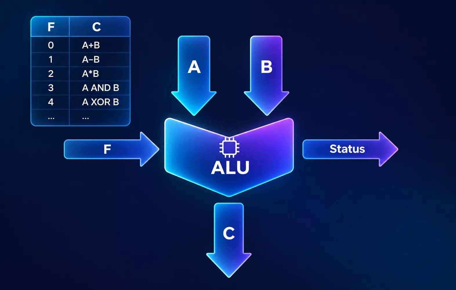
We'll start with arithmetic instructions since they are the easiest to understand. These types of instructions are fed into an Arithmetic Logic Unit (ALU) for processing. An ALU is a circuit that typically takes two inputs with a control signal and outputs a result.
Imagine a basic calculator you used in middle school. To perform an operation, you type in the two input numbers as well as what type of operation you want to perform. The calculator does the computation and outputs the result.
In the case of our CPU's ALU, the type of operation is determined by the instruction's opcode and the control unit would send that to the ALU. In addition to basic arithmetic, ALUs can also perform bitwise operations like AND, OR, NOT, and XOR. The ALU will also output some status info for the control unit about the calculation it has just completed. This could include things like whether the result was positive, negative, zero, or had an overflow.
That's a big part of why modern CPUs are so much faster than older ones running at similar clock speeds.
A modern CPU core doesn't have just one ALU. High-end designs have half a dozen or more integer ALUs working in parallel, plus separate units for floating-point math and vector instructions, which can apply the same operation to a whole batch of numbers at once. That's a big part of why modern CPUs are so much faster than older ones running at similar clock speeds.
An ALU is most associated with arithmetic operations, but it may also be used for memory or branch instructions. For example, the CPU may need to calculate a memory address given as the result of a previous arithmetic operation.
It may also need to calculate the offset to add to the program counter that a branch instruction requires. Something like "if the previous result was negative, jump ahead 20 instructions." In modern CPUs, memory address calculations are usually handed off to dedicated "AGUs" or Address Generation Units, but the principle is the same.
Memory and the Cache Hierarchy
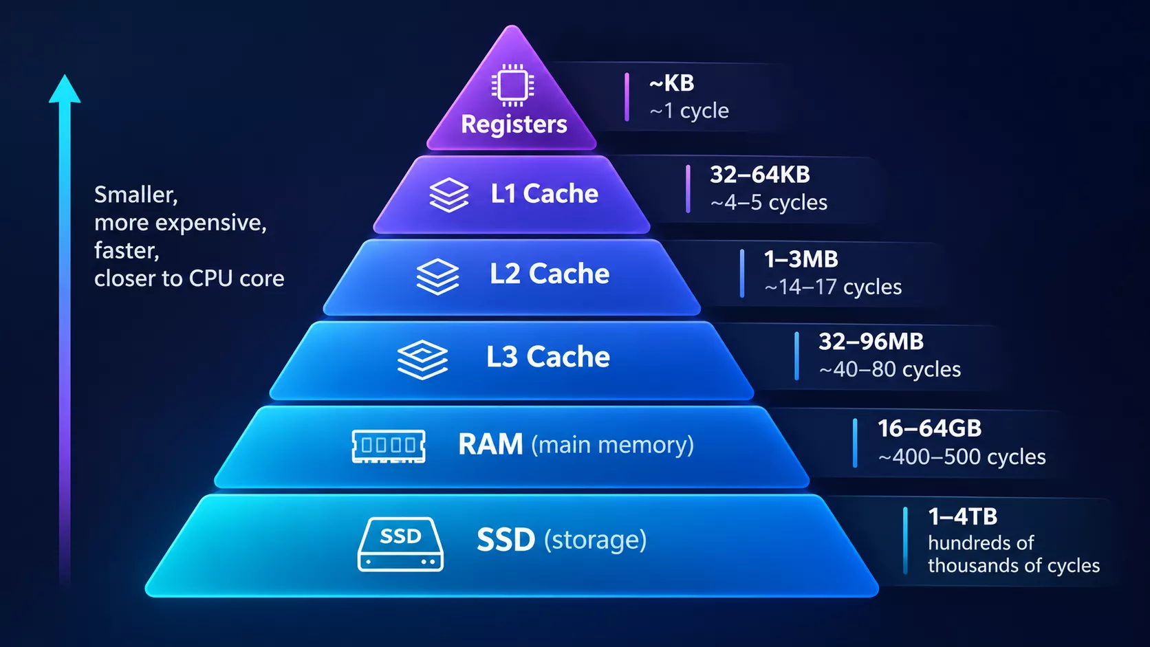
For memory instructions, we'll need to understand a concept called the Memory Hierarchy. This represents the relationship between caches, RAM, and main storage.
When a CPU receives a memory instruction for a piece of data that it doesn't yet have locally in its registers, it will go down the memory hierarchy until it finds it. Most modern CPUs contain three levels of cache: L1, L2, and L3, and some recent designs add a fourth.
The first place the CPU will check is the L1 cache. This is the smallest and fastest level. The L1 cache is typically split into a portion for data and a portion for instructions. Remember, instructions need to be fetched from memory just like data.
A typical L1 cache is tiny, usually 32 to 64KB each for data and instructions per core. If the CPU can't find what it's looking for in the L1 cache, it will check the L2 cache. This is usually 1 to 3MB per core on current desktop chips.
The next step is the L3 cache, which may be a few tens of MB and is shared between cores. AMD's X3D chips stack an extra 64MB of L3 directly on top of the processor, which is why they're so strong in games, a workload that benefits greatly from more cache.
If the CPU can't find the data it needs in the L3 cache, it will go to RAM. If the data isn't in RAM either, the operating system has to load it from storage, which is far slower still. As we go down each step, the available space increases by roughly an order of magnitude, but so does the latency.
Once the CPU finds the data, it will bring it up the hierarchy so that the CPU has fast access to it if needed in the future. There are a lot of steps here, but it ensures that the CPU has fast access to the data it needs.
For example, the CPU can read from its internal registers in just a cycle or two, L1 in a handful of cycles, L2 in a dozen or more, and the L3 in a few dozen. Going out to RAM takes several hundred cycles, and fetching from an SSD takes hundreds of thousands. A hard drive can take millions.
Each core typically has its own private L1 and L2 caches, while the L3 is shared among a group of cores, such as the eight cores on one of AMD's Zen 5 chiplets. Intel's efficiency cores are an exception, sharing an L2 cache in clusters of four. We'll talk more about multi-core CPUs later in this article.
Branches, Pipelining and Prediction
The last of the three major instruction types is the branch instruction. Modern programs jump around all the time and a CPU will rarely ever execute more than a dozen contiguous instructions without a branch.
Branch instructions come from programming elements like if-statements, for-loops, function calls, and return-statements. These are all used to interrupt the program execution and switch to a different part of the code. There are also jump instructions, which are branch instructions that are always taken.
Conditional branches are especially tricky for a CPU since it may be executing multiple instructions at once and may not determine the outcome of a branch until after it has started on subsequent instructions.
In order to fully understand why this is an issue, we'll need to take another diversion and talk about pipelining. Each step in the instruction cycle may take a few cycles to complete. That means that while an instruction is being fetched, the ALU would otherwise be sitting idle. To maximize a CPU's efficiency, we overlap the stages of different instructions in a process called pipelining.
The classic way to understand this is through an analogy to doing laundry. You have two loads to do and washing and drying each take an hour. You could put the first load in the washer and then the dryer when it's done, and then start the second load. This would take four hours. However, if you divided the work and started the second load washing while the first load was drying, you could get both loads done in three hours.
The one-hour reduction scales with the number of loads you have and the number of washers and dryers. It still takes two hours to do an individual load, but the overlap increases the total throughput from 0.5 loads/hr to about 0.67 loads/hr, and with enough loads it approaches one load per hour.
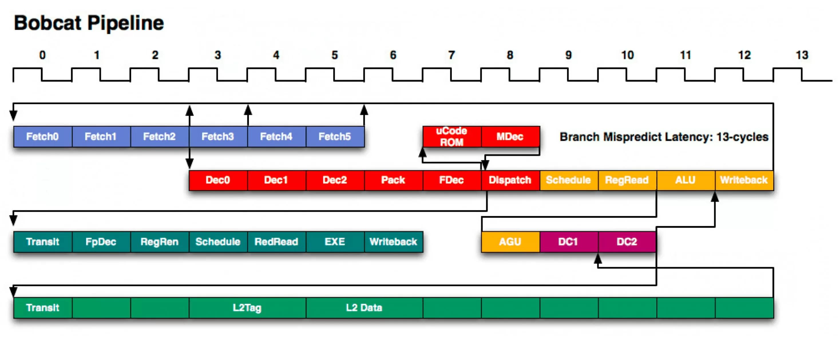
The pipeline of AMD's low-power Bobcat core from 2011. Even a relatively simple design like this one has more than a dozen stages.
CPUs use this same method to improve instruction throughput. A modern Arm or x86 core typically has somewhere between 10 and 20 pipeline stages. And because modern cores also handle several instructions per stage and execute them out of order, a high-end core can have hundreds of instructions in flight at any given moment. Each design is unique, but one sample division may be 4 cycles for fetch, 6 cycles for decode, 3 cycles for execute, and 7 cycles for writing back the results and retiring the instruction.
Back to branches, hopefully you can start to see the issue. If we don't know that an instruction is a branch until cycle 10, we will have already started executing 9 new instructions that may be invalid if the branch is taken. To get around this issue, CPUs have very complex structures called branch predictors.
Some even borrow techniques from machine learning, such as simple neural networks called perceptrons, to guess whether a branch will be taken or not. The intricacies of branch predictors are well beyond the scope of this article, but on a basic level, they track the status of previous branches to learn whether or not an upcoming branch is likely to be taken.
Modern branch predictors are right well over 95% of the time on typical code, and they work so far ahead that they often guess where a program is going before the branch instruction has even been decoded.
Once the result of the branch is known for sure (it's finished that stage of the pipeline), the program counter will be updated and the CPU will go on to execute the next instruction. If the branch was mispredicted, the CPU will throw out all the instructions after the branch that it mistakenly started to execute and start up again from the correct place.
With so many instructions in flight, each wrong guess wastes a lot of work, which is why chipmakers keep pouring transistors into better predictors.
Out-of-Order Execution
Now that we know how to execute the three most common types of instructions, let's take a look at some of the more advanced features of a CPU. Virtually all modern processors don't actually execute instructions in the order in which they are received.
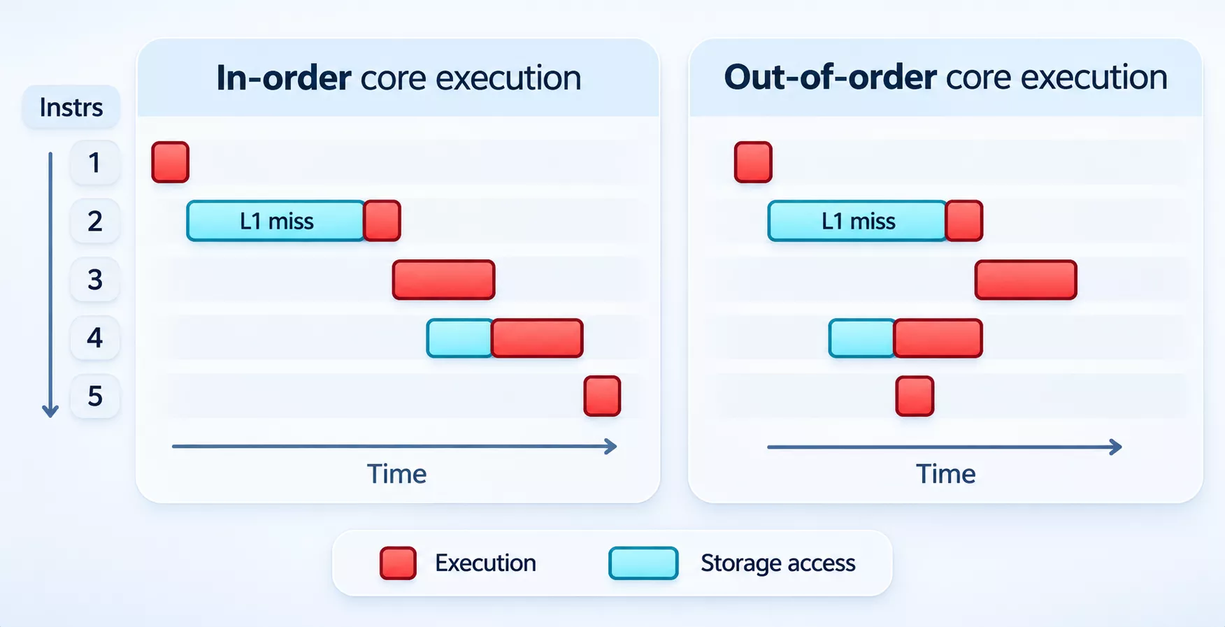
A paradigm called out-of-order execution is used to minimize downtime while waiting for other instructions to finish.
If a CPU knows that an upcoming instruction requires data that won't be ready in time, it can switch the instruction order and bring in an independent instruction from later in the program while it waits. To keep this from breaking the program, the CPU tracks every instruction in a structure called the reorder buffer.
Instructions can finish in any order, but their results are only made final ("retired") in the original program order, so from the software's point of view, everything happened exactly as written. This is also where the register renaming we mentioned earlier pays off, letting independent instructions run side by side without stepping on each other's values. This instruction reordering is an extremely powerful tool, but it is far from the only trick CPUs use.
Another performance improving feature is called prefetching. If you were to time how long it takes for a random instruction to complete from start to finish, you'd find that the memory access takes up most of the time. A prefetcher is a unit in the CPU that watches the pattern of memory accesses and tries to predict what data the program will need next.
If a program is reading through memory in a predictable way, such as stepping through a large array, the prefetcher will reach out to RAM and pull that data into the cache before it's requested. Hence the name pre-fetch.
Speculative Execution and Security
Branch prediction and out-of-order execution have a side effect worth knowing about. When a CPU guesses which way a branch will go, it doesn't just fetch those instructions. It executes them speculatively and throws the results away if the guess was wrong. For decades, that was considered harmless.
That changed in 2018 with the disclosure of Spectre and Meltdown, two families of vulnerabilities that showed discarded speculative work still leaves traces behind, mainly in the cache. By carefully measuring how long memory accesses take, an attacker could infer data the CPU was never supposed to reveal, such as passwords or encryption keys from another program. Virtually every high-performance CPU from Intel, AMD and Arm was affected to some degree.
Meltdown has since been fixed in hardware, but Spectre-style attacks are a whole class of problems rather than a single bug, and new variants continue to surface every year.
Chipmakers now design their cores with these side channels in mind, and some of the software mitigations come with a performance cost. It's a good example of how the same features that make modern CPUs fast can also make them harder to secure.
Accelerators and AI
Another major feature now routinely included in CPUs is task-specific accelerators. These are circuits whose entire job is to perform one small task as fast as possible. This might include encryption, media encoding, or machine learning.
The CPU can do these things on its own, but it is vastly more efficient to have a unit dedicated to them. A great example of this is graphics. Surely the CPU can perform the computations needed for graphics processing, but having a dedicated unit for them (an integrated GPU) offers orders of magnitude better performance.
A big addition in recent years is the NPU, or Neural Processing Unit, a block built specifically to run AI workloads like live transcriptions or local language models while sipping power. NPUs went from virtually nonexistent in PCs to a near-standard feature in just a couple of years.
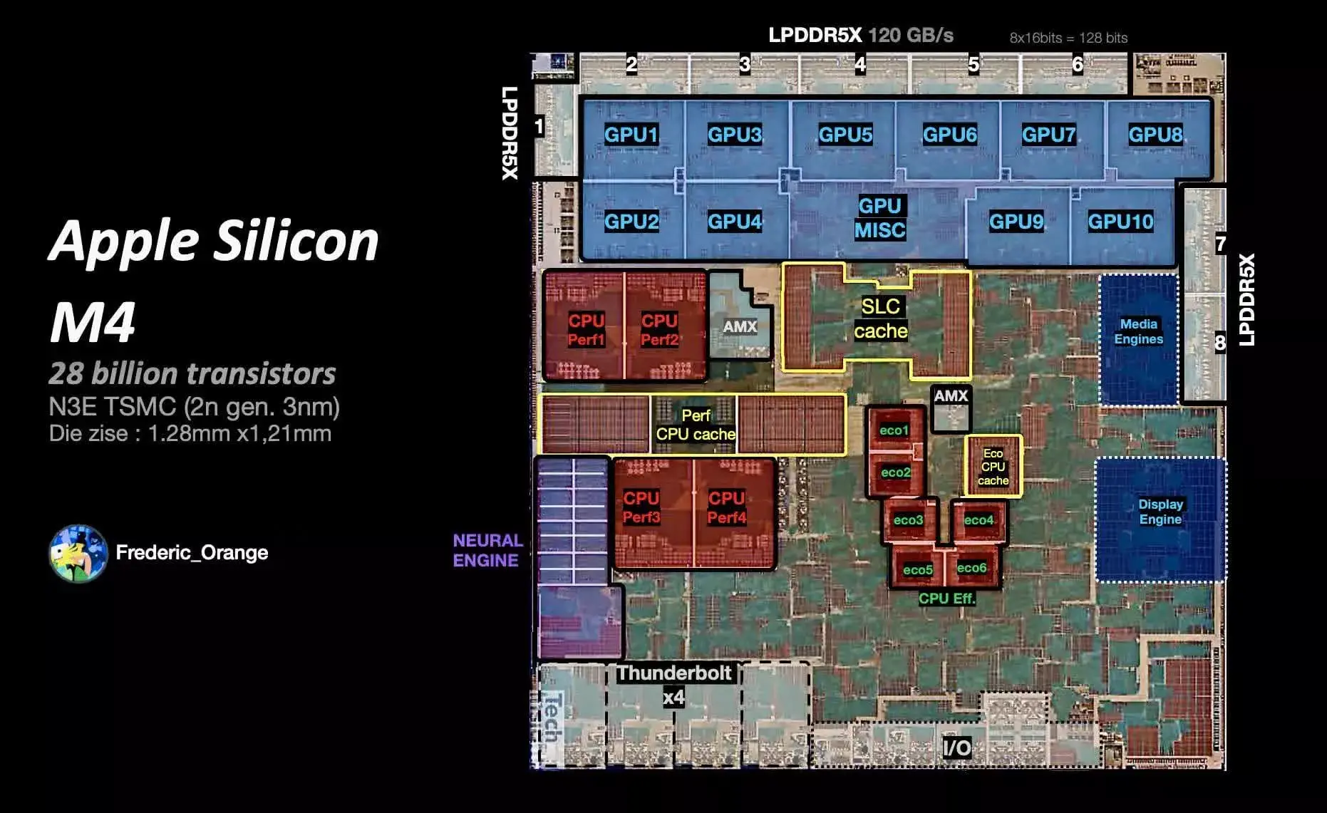
The CPU cores themselves have also gained more specialized hardware. Wide vector extensions like AVX-512 can crunch 16 numbers in a single instruction, and newer matrix extensions, such as Intel's AMX on server chips and Arm's SME found in Apple's M4, are designed specifically to accelerate AI math.
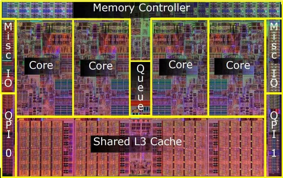
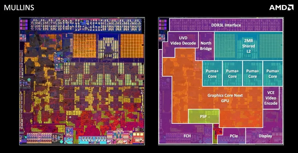
The picture below shows an Intel CPU from 2008. Most of the space is taken up by cores and cache. The second picture shows an AMD "Mullins" mobile APU. Most of the space there is taken up by components other than the cores.
Above: the die of Intel's first generation Nehalem architecture. Note that the cores and cache take up the majority of the space. Below: The die of an AMD SoC showing the large amount of space devoted to accelerators and external interfaces.
Dedicated media engines handle video encoding and decoding, including the AV1 codec, so recording or streaming barely touches the cores.
With the rise of accelerators, the CPU cores may only take up a fraction of the chip, especially in laptop processors where the GPU, NPU and media engines are all integrated alongside them.
Going Multicore
The last major feature to cover is how we can connect a bunch of individual CPUs together to form a multicore CPU. It's not as simple as just putting multiple copies of the single core design we talked about earlier. Just like there's no easy way to turn a single-threaded program into a multi-threaded program, the same concept applies to hardware. The issues come from dependence between the cores.
The cores don't each get their own path to RAM. Instead, they're linked by an on-chip interconnect, such as a ring or a mesh, that connects them to each other, to the shared L3 cache, and to the memory controllers.
With multiple entities operating on potentially the same pieces of data, issues like coherence and consistency must be resolved. If two cores were both processing instructions that used the same data, how do they know who has the right value? What if one core modified the data but it didn't reach the other core in time for it to execute? Since they have separate caches that may store overlapping data, complex algorithms and controllers must be used to remove these conflicts.
Typically, separate cores will process instruction streams from different threads. This helps reduce the dependence between cores. That's why if you check Task Manager, you'll often see a few cores working hard while the others are hardly working. Many programs still aren't designed for multithreading, or only split their work across a handful of threads. There may also be certain cases where it's more efficient to have one core do the work rather than pay the overhead penalties of trying to divide up the work.
Simultaneous Multithreading
Many CPUs also let a single core work on two threads at once, a technique called simultaneous multithreading (SMT), which Intel brands as Hyper-Threading. Since even the best out-of-order core can't keep all of its execution units busy all the time, a second thread can fill in the gaps.
It typically adds 10 to 30% more throughput in well-threaded workloads for very little extra die space. SMT has long been a staple of modern CPUs, but Intel recently dropped Hyper-Threading from the performance cores in its Lunar Lake and Arrow Lake chips, opting to spend that effort on making each core faster and more efficient instead. Apple and Qualcomm don't use SMT at all.
Hybrid Architectures
For years, every core in a desktop CPU was identical. That's no longer a given. Borrowing the idea from how smartphone chips work, many processors mix large and fast performance cores (usually referred to as P-cores) with smaller and more power-efficient cores (E-cores).
Some recent laptop chips add a third tier of low-power cores for light background tasks as well. Intel adopted this approach with Alder Lake in 2021, and Apple and Qualcomm do something similar. Meanwhile, AMD builds compact "c" versions of its Zen cores that trade peak clock speed for size and efficiency.
The catch is that the operating system needs to know which core is best for which job. Intel's Thread Director, for example, feeds hints to Windows about what each thread is doing, so a game lands on the P-cores while background updates are sent to the E-cores.
Chiplets and Tiles
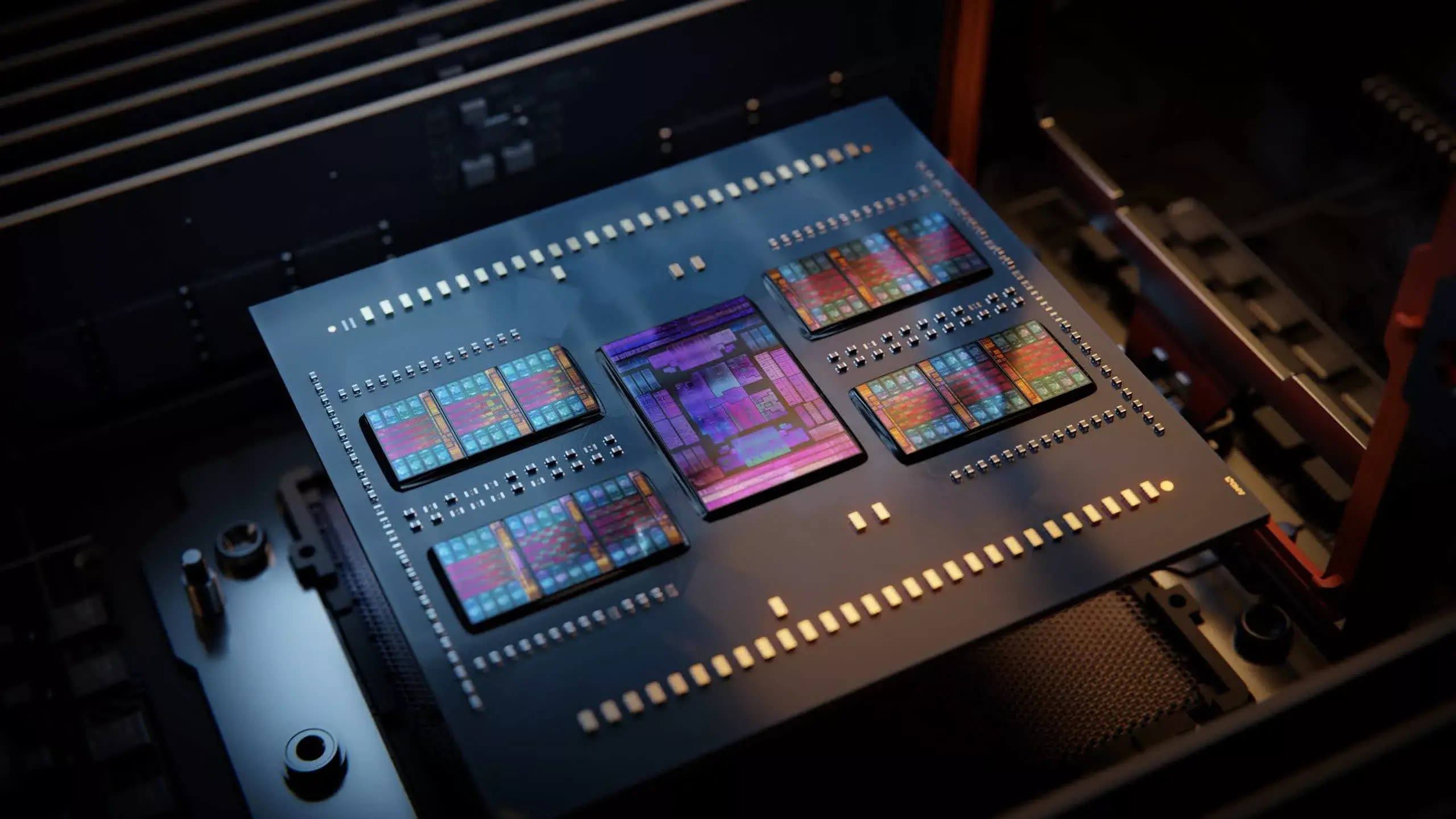
The other big shift is in how CPUs are physically built. We wrote an entire technical explainer about the importance of chiplets a while back. The idea is that instead of making one large piece of silicon, both AMD and Intel now split their processors into smaller dies, which AMD calls chiplets and Intel calls tiles, and connect them inside the same package.
For example, a Ryzen 9 9950X combines two 8-core compute chiplets with a separate I/O die that handles memory, PCIe and USB.
Smaller dies are cheaper to make, since a single defect ruins less silicon, and each piece can be built on whatever manufacturing process suits it best. The trade-off is communication: data traveling between chiplets takes longer than data staying on one die, which is why software and schedulers sometimes need to keep related threads on the same chiplet.
Advanced packaging techniques like Intel's Foveros and AMD's 3D V-Cache go a step further by stacking dies on top of each other.
Physical Design: From Blueprint to Silicon
Most of this article has focused on the architectural design of a CPU since that's where most of the complexity is. However, this all needs to be created in the real world and that adds another level of complexity.
In order to synchronize all the components throughout the processor, a clock signal is used. Modern desktop processors typically run between 3GHz and 5GHz, with the fastest chips boosting to around 6GHz or more. That's a modest increase over the past decade, as most of the performance gains have come from elsewhere. At each of these cycles, the billions of transistors inside a chip are switching on and off.
Clocks are critical to ensure that as each stage of the pipeline advances, all the values show up at the right time. But clock speed alone doesn't determine how fast a CPU is.
Performance comes down to clock speed multiplied by how many instructions the core can complete per clock cycle (IPC). Everything we've covered, from wider decoders and multiple ALUs to bigger caches and better branch predictors, exists to raise IPC. That's why a modern core running at 5GHz is several times faster than one from a decade ago running at a similar speed.
Everything we've covered, from wider decoders and multiple ALUs to bigger caches and better branch predictors, exists to raise IPC.
Increasing the clock frequency through overclocking will make the chip faster, but will also increase power consumption and heat output. These days, CPUs handle most of that on their own. Boost algorithms constantly adjust clock speeds and voltages based on temperature, power draw and workload, pushing each chip close to its limits right out of the box and without any manual intervention. That leaves far less headroom for manual overclocking than there used to be.
Heat is a CPU's worst enemy, that part hasn't changed. Modern chips are designed to run hot, and they automatically throttle their clocks if they reach their temperature limit, typically around 95 to 105°C. Long-term damage comes from the combination of heat, voltage and current, which slowly wears down the microscopic transistors and wiring.
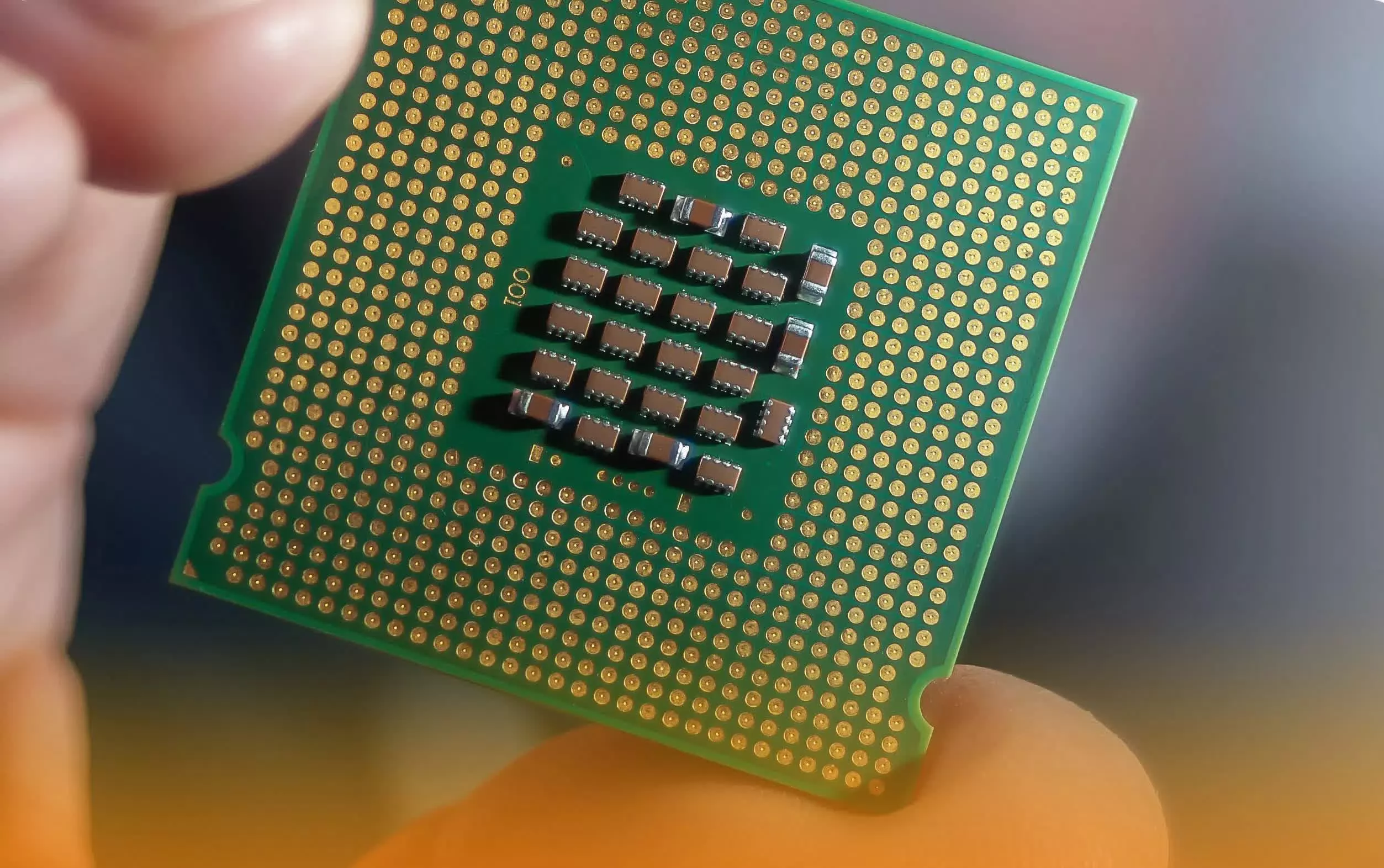
This is why desktop CPUs come with heat spreaders. The actual silicon dies of a CPU may only take up 20% of the surface area of a physical device. Increasing the footprint allows the heat to be spread more evenly to a heatsink. It also allows more contacts for interfacing with external components.
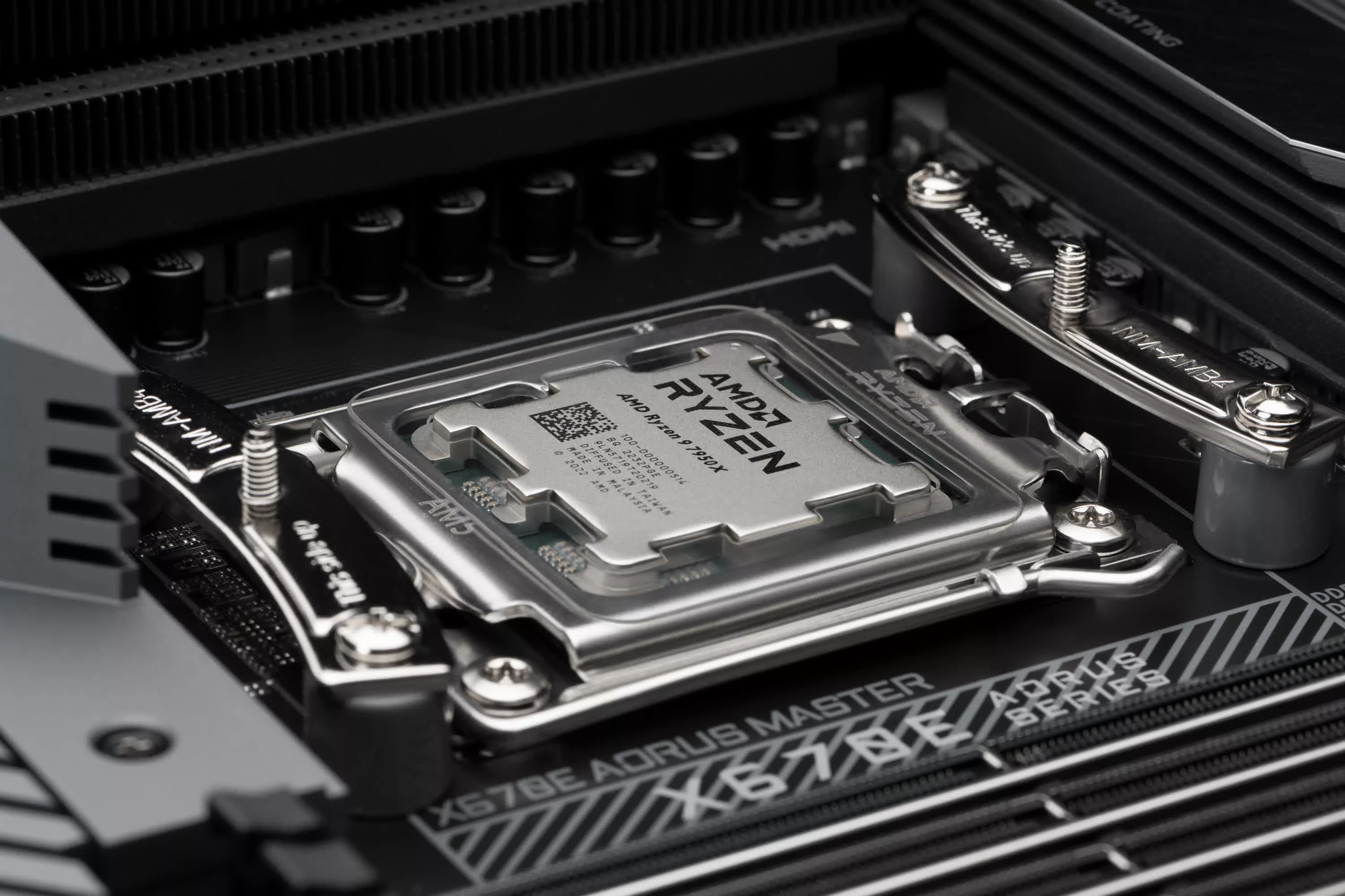
Modern desktop CPUs have well over a thousand electrical contacts on the back. AMD's AM5 socket uses 1,718 and Intel's LGA 1851 socket uses 1,851. Both now use the LGA design, where the CPU has flat pads and the pins are in the motherboard socket instead.
Laptop chips are soldered directly to the motherboard using a grid of tiny solder balls, often numbering well over a thousand as well. Regardless of the design, around half of them are devoted to power delivery and the rest are used for data. This includes communication with the RAM, chipset, storage, PCIe devices, and more.
With high-performance CPUs drawing upwards of 200 amps at full load, they need hundreds of contacts to spread out the current draw evenly. The contacts are usually gold plated to improve electrical conductivity. Different manufacturers use different arrangements of contacts throughout their many product lines.
The transistors themselves keep shrinking and changing shape, too. The latest manufacturing processes from TSMC and Intel are moving from FinFET transistors to gate-all-around designs, where the gate fully wraps the channel for better control and less leakage. Intel's 18A process, used in its Panther Lake chips, also introduces backside power delivery, which moves the power wiring to the back of the silicon wafer and leaves the front free for data signals. For a much deeper look at how chips are manufactured, check out Part 3 of our CPU design series.
Putting It All Together: Inside AMD's Zen 5
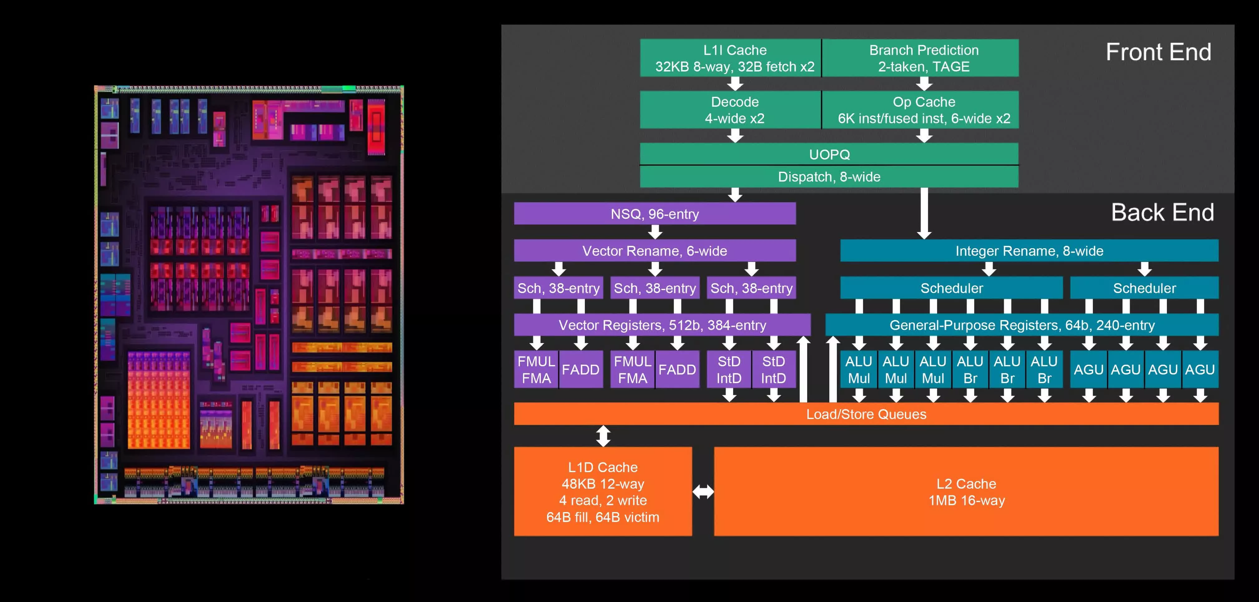
To wrap things up, we'll take a quick look at the design of a modern CPU core: AMD's Zen 5, found in the Ryzen 9000 series. AMD has published detailed diagrams of the core, and nearly every concept we've covered shows up in it.
Starting at the top, the branch predictor runs ahead of everything else, guessing where the program is headed and telling the front end which instructions to fetch. Those instructions come from a 32KB L1 instruction cache, with help from the TLB buffer, a small cache that remembers recent translations between the memory addresses a program uses and their actual physical locations in RAM.
From there, the instructions go through two separate decode clusters that work in parallel, each turning x86 instructions into micro-ops. Code that has run recently can skip decoding entirely and come straight out of the micro-op cache. Either way, up to eight micro-ops per cycle are passed along to the next stage.
AMD's Zen 5 core, as used in Ryzen 9000 desktop processors
This is where the out-of-order machinery takes over. The micro-ops go through register renaming and are entered into a 448-entry reorder buffer, which tracks every instruction. They then wait in schedulers until their input data is ready. The exact workings of these are a bit complex (think graduate-level university course), but they are what let the core pick the most timely instruction to execute next while keeping results in the correct order.
Once an instruction is ready, it's sent to one of the execution units. Zen 5 has six integer ALUs, four address generation units for memory operations, and a floating-point and vector unit that can process full 512-bit AVX-512 instructions. Memory operations are served by a 48KB L1 data cache, backed by a 1MB L2 cache per core and a 32MB L3 shared by all eight cores on the chiplet.
The output results will be stored, the instruction will be retired in program order, and the CPU is now ready to start on the next instruction. That's about it!
While this article was not meant to be a definitive guide to exactly how every CPU works, it should give you a good idea of their inner workings and complexities (!). Frankly, no one outside of Intel, AMD or Apple knows every detail of how their CPUs work. Each section of this article represents an entire field of research and development so the information presented here just scratches the surface.
Keep Reading
If you are interested in learning more about how the various components covered in this article are designed, check out Part 2 of our CPU design series. If you're more interested in learning how a CPU is physically made down to the transistor and silicon level, check out Part 3.