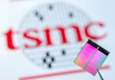
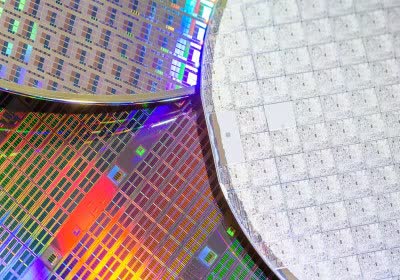
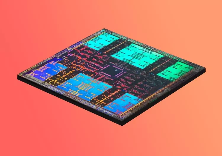
The big picture: The semiconductor industry is approaching a significant milestone as TSMC prepares to expand the physical scale of its chip packaging technology. At its recent North American Technology Symposium, the company detailed plans for a new generation of CoWoS (Chip-on-Wafer-on-Substrate) technology, enabling the assembly of multi-chiplet processors much larger than those currently in production.
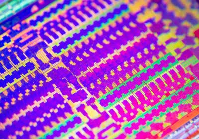
Forward-looking: Researchers at the University of Massachusetts Amherst have developed a laser-based technique to align 3D semiconductor chips, potentially overcoming a longstanding challenge in chip manufacturing. The method employs concentric metalenses to generate holograms that reveal misalignment between chip layers at a much smaller scale than previously possible.
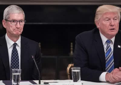
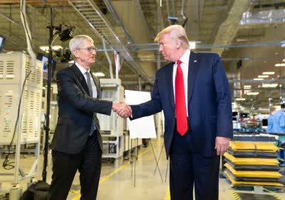
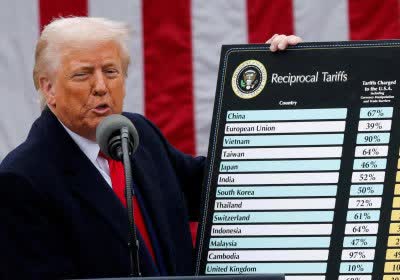
In context: President Trump's 104% tariff on goods imported from China is now in effect. It will have an enormous impact on many US firms, especially Apple, which relies heavily on China to manufacture its iPhones. Trump believes the solution is to start making the handsets in the US, but that would be nearly impossible, especially in the short term. And even if it were, iPhones would likely become much more expensive.
A hot potato: TSMC has repeatedly said that funding a new chip-making venture outside Taiwan is very expensive for numerous reasons. However, a new analysis tries to debunk the company's alleged financial issues with building new plants in other parts of the world.