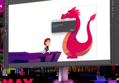
Adobe wows with Project Turntable, an AI tool that rotates 2D art in 3D space
Yet another MAX event packed with generative AI tools
S3 Graphics: Gone But Not Forgotten
#TBT These days it's rare to see a new hardware company break ground in the world of PCs, but 30 years ago, they were popping up all over the place. Join us as we pay tribute to S3 and see how its remarkable story unfolded over the years.

See what these 3D games would look like if they were in 2D
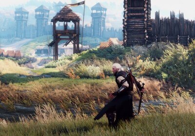
The joy of free-camera screenshots